
SLIDE 1
www.microstencil.com/stencil.html www.microstencil.com/stencil.html www.microstencil.com/stencil.html www.microstencil.com/stencil.html
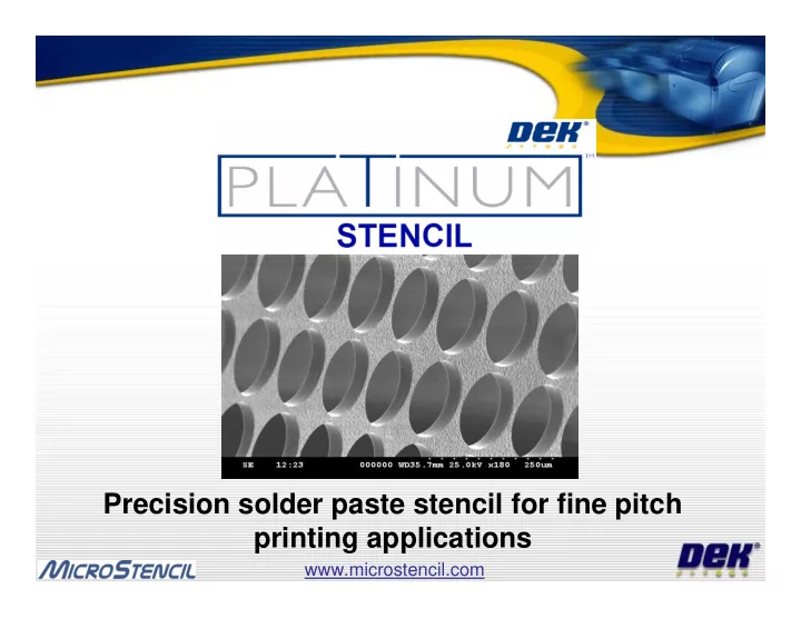
Precision solder paste stencil for fine pitch printing applications
www.microstencil.com
Precision solder paste stencil for fine pitch printing applications - - PowerPoint PPT Presentation
www.microstencil.com/stencil.html www.microstencil.com/stencil.html www.microstencil.com/stencil.html www.microstencil.com/stencil.html Precision solder paste stencil for fine pitch printing applications www.microstencil.com Overview A
www.microstencil.com/stencil.html www.microstencil.com/stencil.html www.microstencil.com/stencil.html www.microstencil.com/stencil.html
www.microstencil.com
semiconductor fabrication processes techniques
applications and other fine pitch or high yield printing requirements
www.microstencil.com
www.microstencil.com
50m pitch 45m diameter circular apertures 60m pitch 30m diameter circular apertures
Stencil apertures examples– SEM images
7.5 µm diameter circular aperture 175 micron diameter aperture 225 micron pitch 100 micron diameter aperture
www.microstencil.com
www.microstencil.com
www.microstencil.com
1000 times magnification
– Smooth squeegee side of stencils inhibits fine PSD solder pastes smearing on stencil surface during printing therefore allowing a lower print pressure. – Smooth substrate side improves the seal during printing onto wafers and allows an effective underside stencil cleaning process
0.53mm
– Squeegee side
– Board side
– Note: Stainless steel 220HV
Interferometer surface scan
www.microstencil.com
– In addition a smooth underside of the stencil can enable on- printer cleaning techniques not normally possible with conventional E-form stencils for wafer level printing
www.microstencil.com
design area
– <3 µm for 50 µm thick stencils – 4 µm for 50-100 µm thick stencils – 6 µm for 100-200 µm thick stencils – 8 µm for 200-230 µm thick stencils
www.microstencil.com
www.microstencil.com
Electroformed nickel apertures 35µmx 80µm at 60µm pitch. Stencil thickness: 20µm Developmental type 8 paste. Powder size range 2-8µm. Print deposits at 60µm pitch. Wafer printing at 60µm pitch with type 8 paste.
Wafer printing - 60 micron pitch, 6-inch wafer (images courtesy of Technical University of Berlin)
Ref:erence:
advancements in stencil printing processes for Ultra-fine-pitch flip chip bumping down to 60µm pitch”, IMAPS San Diego, Ca, 2006 Wafer printing at 60µm pitch with type 8 paste.
www.microstencil.com
Case Study – 60 micron pitch 6-inch wafer bumping (images courtesy of Technical University of Berlin)
. Bump height distribution at 60µm pitch, Average height: 28µm Shear mode for bumps at 60µm Pitch, fracture
Cross section of bumped chip at 60µm pitch.
Ref:erence:
advancements in stencil printing processes for Ultra-fine-pitch flip chip bumping down to 60µm pitch”, IMAPS San Diego, Ca, 2006
www.microstencil.com
www.microstencil.com
Cheif Technical Officer 115A Commonwealth Drive, #04-01, Singapore, 149596 Main Line: +65 6484 7010 Direct Dial: +65 6419 5852 Email: r.w.kay@microstencil.com Internet: www.microstencil.com MicroStencil Ltd, 13 Ladysneuk Rd, Stirling, UK General enquires: sales@microstencil.com DEK Printing Machines Ltd, 11 Albany Road, Granby Industrial Estate, UK www.microstencil.com