
Originally published in the Proceedings of SMTA International, Ft. Worth, TX, October, 2013
STENCIL AND SOLDER PASTE INSPECTION EVALUATION FOR MINIATURIZED SMT COMPONENTS
Robert Farrell Benchmark Technologies Nashua, NH USA Chrys Shea Shea Engineering Services Burlington, NJ USA
ABSTRACT New stencil materials and manufacturing technologies promise improved performance over traditional options. To determine the best technologies for a contract electronics manufacturer assembling miniaturized SMT components, a test was designed to assess the performance of 11 different stencils, submitted by 3 different suppliers, using a variety of materials and
- coatings. Performance metrics include print volume
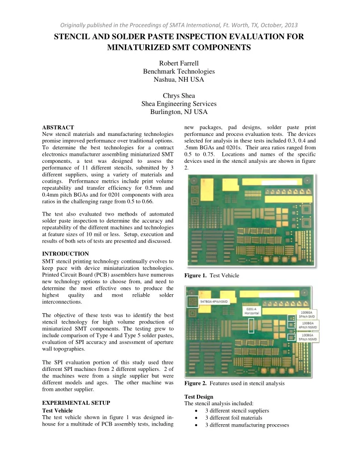
repeatability and transfer efficiency for 0.5mm and 0.4mm pitch BGAs and for 0201 components with area ratios in the challenging range from 0.5 to 0.66. The test also evaluated two methods of automated solder paste inspection to determine the accuracy and repeatability of the different machines and technologies at feature sizes of 10 mil or less. Setup, execution and results of both sets of tests are presented and discussed. INTRODUCTION SMT stencil printing technology continually evolves to keep pace with device miniaturization technologies. Printed Circuit Board (PCB) assemblers have numerous new technology options to choose from, and need to determine the most effective ones to produce the highest quality and most reliable solder interconnections. The objective of these tests was to identify the best stencil technology for high volume production of miniaturized SMT components. The testing grew to include comparison of Type 4 and Type 5 solder pastes, evaluation of SPI accuracy and assessment of aperture wall topographies. The SPI evaluation portion of this study used three different SPI machines from 2 different suppliers. 2 of the machines were from a single supplier but were different models and ages. The other machine was from another supplier. EXPERIMENTAL SETUP Test Vehicle The test vehicle shown in figure 1 was designed in- house for a multitude of PCB assembly tests, including new packages, pad designs, solder paste print performance and process evaluation tests. The devices selected for analysis in these tests included 0.3, 0.4 and .5mm BGAs and 0201s. Their area ratios ranged from 0.5 to 0.75. Locations and names of the specific devices used in the stencil analysis are shown in figure 2. Figure 1. Test Vehicle Figure 2. Features used in stencil analysis Test Design The stencil analysis included: 3 different stencil suppliers 3 different foil materials 3 different manufacturing processes