THE EFFECTS OF STENCIL ALLOY AND CUT QUALITY ON SOLDER PASTE PRINT - - PDF document

the effects of stencil alloy and cut quality on solder
SMART_READER_LITE
LIVE PREVIEW

THE EFFECTS OF STENCIL ALLOY AND CUT QUALITY ON SOLDER PASTE PRINT - - PDF document

Originally published in the Proceedings of SMTA International, September, 2014 THE EFFECTS OF STENCIL ALLOY AND CUT QUALITY ON SOLDER PASTE PRINT PERFORMANCE Chrys Shea Shea Engineering Services Burlington, NJ USA Ray Whittier Vicor


slide-1
SLIDE 1

Originally published in the Proceedings of SMTA International, September, 2014

THE EFFECTS OF STENCIL ALLOY AND CUT QUALITY ON SOLDER PASTE PRINT PERFORMANCE

Chrys Shea Shea Engineering Services Burlington, NJ USA Ray Whittier Vicor Corporation – VI Chip Division Andover, MA USA

ABSTRACT The stencil is a key factor in the solder paste printing process, and many characteristics influence its performance. This study uses a designed experiment to vary two key stencil characteristics: alloy and cut quality. The experimental matrix directly compares the current best- in-class stainless steel alloy with a new experimental foil material designed for higher tension. Cut qualities are naturally varied by producing the stencils at six different suppliers in each of three global regions, creating a total of twelve individual test specimens. The tests use a common, very high density production PCB as a test vehicle. Identical print performance experiments are performed. Response variables include print yields, transfer efficiencies and volume repeatabilities using the established ten-print test

  • method. Performance results are compared with the

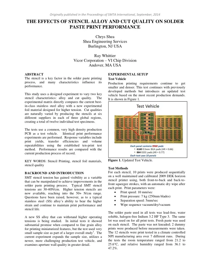
current production process of record. KEY WORDS: Stencil Printing, stencil foil materials, stencil quality BACKROUND AND INTRODUCTION SMT stencil tension has gained visibility as a variable that can be manipulated to achieve improvements in the solder paste printing process. Typical SMT stencil tensions are 30-40N/cm. Higher tension stencils are now available, reaching into the 50+ N/cm range. Questions have been raised, however, as to a typical stainless steel (SS) alloy’s ability to bear the higher strain and continue to maintain print performance and stencil life. A new SS alloy that can withstand higher operating tensions is being studied. In initial tests it showed substantial promise when compared to fine grain alloy for printing miniaturized features, but the test used very small sample size as part of a larger overall study1. The current experiment expands the sample size, utilizes a newer, more challenging production test vehicle, and examines aperture wall quality in greater detail. EXPERIMENTAL SETUP Test Vehicle Production printing requirements continue to get smaller and denser. This test continues with previously developed methods but introduces an updated test vehicle based on the most recent production demands. It is shown in Figure 1. Figure 1. Updated Test Vehicle. Test Methods For each stencil, 10 prints were produced sequentially

  • n a well maintained and calibrated 2009 DEK horizon

stencil printer using, both front-to-back and back-to- front squeegee strokes, with an automatic dry wipe after each print. Print parameters were:  Print speed: 10 mm/sec  Print pressure: 7 kg (250mm blades)  Separation speed: 5mm/sec  Wipe sequence vacuum/dry/vacuum The solder paste used in all tests was lead-free, water soluble, halogen-free Indium 3.2 HF Type 3. The same lot was used on for all print tests. Fresh paste was used

  • n each stencil. The paste was not kneaded; 2 dummy

prints were produced before measurements were taken. The 12 stencils were print tested in a climate controlled NPI manufacturing area over 7 different runs. During the tests the room temperature ranged from 21.2 to 25.6°C, and relative humidity ranged from 36.1 to 47.2%.

slide-2
SLIDE 2

Originally published in the Proceedings of SMTA International, September, 2014 The PCB was supported with a flat, non-vacuum tooling plate and edge clamps. Deposit volume measurements were taken with a Koh Young 3020VAL using a Bare Board Teach to set the reference plane. Test Matrices 6 suppliers from 3 different global regions each cut 2

  • stencils. The 2 foils were different stainless steel alloys

that were mesh mounted onto rigid tubular aluminum frames.  Alloy F was fine grain stainless steel (FG) mounted at standard (39 N/cm) tension  Alloy T the other was the experimental alloy with a higher tensile strength Both were 4mil (100µm) thick, and mounted at standard (39 N/cm) tension/ The foils were mounted and tensioned by the material supplier prior to shipment to the stencil vendors for cutting. A total of 12 stencils were tested in their as-received

  • condition. No nanocoatings or other treatments were
  • applied. It should be noted that the production Process
  • f Record (POR) uses a second-generation SAMP-

based nanocoating on a fine grain SS foil. An additional 4 test stencils were added to evaluate the effect of electropolishing from one of the suppliers and to provide internal benchmarking for a local supplier. They were not analyzed as completely as the primary test stencils in this study. The expanded test matrix is shown in Table 1. Table 1. DOE Matrix RESULTS AND DISCUSSION Aperture Measurements To calculate actual transfer efficiencies and area ratios, the stencils’ apertures and thicknesses were measured. Their specifications are as follows:  Circular microBGA apertures: 10.8mil  Rectangular 0201 apertures: 11.8x13.8mil  Foil thickness: 4mil The apertures were measured on the PCB side with a Keyence VR-3100 digital microscope; 20 of each BGA aperture size were measured per stencil, and 24 of each 0201 aperture size (12 at 0 degree and 12 at 90 degree

  • rientation) were measured per stencil.

Circular BGA apertures averaged 10.4mil diameter. The smallest average aperture was 9.9mils and the largest was 10.7mils. Rectangular 0201 apertures averaged 11.3 x 13.3. Their smallest and largest apertures varied by 0.3mil, for minimums of 11.0 and 13.0 and maximums of 11.0 and 11.6, respectively. Foil thickness were consistent at 4.0mil on the SS due to its precision manufacturing process (>6σ at 2% tolerance). Paste Volume Measurements & Print Yields The actual Area Ratios (ARs) and aperture volumes were calculated using the average aperture size for each

  • stencil. The aperture volumes were then combined with

the average measured solder paste deposit volume to calculate actual transfer efficiencies. The print yields and paste volume information resulting from the 10-print tests are shown in Tables 2 through 4. Stencils that produced 100% yields are highlighted. Table 2. MicroBGA Print Test Results

Stencil # Supplier Region Foil Type 1 A USA F 2 A USA T 3 B USA F 4 B USA T 5 C Asia F 6 C Asia T 7 D Asia F 8 D Asia T 9 E EU F 10 E EU T 11 F EU F 12 F EU T 13 G Local F -SS Frame 14 G Local F - Tube Frame 15 C Asia F - EP 16 C Asia F - Non-EP

Stencil # Alloy Yield Dep Vol AR Ap Vol TE CV - TE 1

F 50%

312 0.67

361 87% 7.9%

2

T

30% 317 0.66 352 90% 7.9% 3

F 50%

320 0.63

323 99% 8.1%

4

T

10% 301 0.62 310 97% 9.9% 5

F 90%

328 0.65 344

95% 8.9%

6

T

80% 329 0.65 338 97% 9.1% 7

F 100%

321 0.66 353

91% 9.0%

8

T

60% 328 0.65 344 95% 9.1% 9

F 90%

330 0.66 349

95% 8.6%

10

T 100%

335 0.65 345

97% 8.8%

11

F 10%

290 0.66 350

83% 9.1%

12

T 100%

341 0.66 346

99% 9.4%

15

F, Epolish 30%

310 0.66 348

89% 8.4%

16

F

60% 310 0.65 338 92% 8.4%

0.5mm BGA Results

slide-3
SLIDE 3

Originally published in the Proceedings of SMTA International, September, 2014 Table 3. Print Test Results for 0201s at 0 degree

  • rientation

Table 4. Print Test Results for 0201s at 90 degree

  • rientation

ANALYSIS 1) Print Yields Print yields are determined by the automatic solder paste inspection system. All 9568 deposits must fall within their specified ranges for the print to be considered a pass. As little as one deposit out-of-spec will cause the print to be a fail. The print yields are show in figure 2. SPI tolerance specifications are as follows:  µBGA: 20% - 139%  0201: 40% - 200%  Other components: 50% - 150% Figure 2. Print yields of different stencils in 10-print test. Stencil suppliers A and B provided the stencils with the lowest yields. Using 80% or better as a benchmark, 6

  • f the remaining 8 stencils met the goal; 5 of them

reached 90% or better, and 3 of them achieved 100%

  • yield. It should be noted that the fine grain stencil from

supplier F, noted with an asterisk, had one aperture clogged though the first 9 runs, which caused the low

  • yield. Every other deposit was within specification.

The blockage on that specific aperture released on the 10th print, and the board passed SPI. The cause of the blockage – whether it was due to solder paste or the stencil manufacturing process – is unknown. The stencil would have shown 100% yield if it weren’t for that specific aperture blockage. In comparison, the current production Process of Record (POR), which yields 97-98% in production. Based on test stencil yields, the three that produced 100% good boards would be considered equivalent; the two that produced 90% yield would also be good candidates for further investigation. 80% yield would be considered a bare minimum for consideration of further investigation. 2) Transfer Efficiencies Transfer efficiencies (TE) are the ratio of the volume of the measured deposit to the volume of the stencil aperture and are expressed as a percent, or, more simply put, the percentage of solder paste that releases from the

  • aperture. The aperture volumes used in the calculations

are computed based on the average measured aperture dimension and stencil thickness, not on their specifications. The most critical transfer efficiencies on this PCB are those of the µBGAs, as they are the smallest feature with a 0.66 AR, and the most populous feature, with

  • ver 6000 per print.

Stencil # Alloy Yield Dep Vol AR Ap Vol TE CV - TE 1

F 50%

606 0.79

638 95% 9.3%

2

T

30% 615 0.79 639 96% 8.8% 3

F 50%

650 0.79

651 100% 8.9%

4

T

10% 614 0.76 593 104% 9.2% 5

F 90%

646 0.76 591

109% 8.9%

6

T

80% 649 0.76 594 109% 9.2% 7

F 100%

622 0.79 650

96% 9.0%

8

T

60% 629 0.78 624 101% 8.9% 9

F 90%

642 0.78 622

103% 8.9%

10

T 100%

647 0.76 591

110% 8.7%

11

F 10%

574 0.77 611

94% 9.4%

12

T 100%

669 0.77 616

109% 10.1%

15

F, Epolish 30%

609 0.77 615

99% 9.5%

16

F

60% 605 0.77 614 99% 9.6%

0201 0° Orientation Results

Stencil # Alloy Yield Dep Vol AR Ap Vol TE CV - TE 1

F 50%

603 0.78

631 95% 9.3%

2

T

30% 611 0.79 640 95% 8.9% 3

F 50%

653 0.79

643 101% 9.1%

4

T

10% 609 0.75 586 104% 9.3% 5

F 90%

703 0.75 582

121% 7.3%

6

T

80% 706 0.75 583 121% 7.7% 7

F 100%

619 0.77 621

100% 9.0%

8

T

60% 628 0.77 618 102% 8.8% 9

F 90%

643 0.78 625

103% 9.3%

10

T 100%

649 0.75 587

111% 9.3%

11

F 10%

573 0.77 609

94% 9.4%

12

T 100%

670 0.77 605

111% 10.4%

15

F, Epolish 30%

609 0.77 614

99% 8.4%

16

F

60% 602 0.76 600 100% 8.4%

0201 90° Orientation Results

slide-4
SLIDE 4

Originally published in the Proceedings of SMTA International, September, 2014 Desired TE’s are 80% or better. 83-85% is typical for this test vehicle in its production process. Figure 3 shows the transfer efficiencies of the test stencils. All

  • f them exceeded the 80% benchmark, with several

achieving 90% or even 100%. It should be noted that excess slag on the bottom side of the apertures can contribute to higher TE numbers by lifting the stencil from the PCB. This situation can produce artificially inflated TE in tests, but induces poor gasketing and

  • verall higher print defects and variation in production.

Therefore, TE alone should not be used as a deciding factor in any stencil selection tests, particularly if PCB contact side topography is not examined. Figure 3 shows that in 5 of the 6 pairs of stencils, the TE of the experimental material exceeded that of the fine grain material for the µBGAs. Note that the stencil pair that did not follow the trend was also the one that produced the lowest yields. Transfer efficiencies for 0201s are shown in Figures 4 and 5. In 11 of 12 pairs of data, the experimental alloy produced TEs equal to or higher than the fine grain SS alloy. Figure 3. Transfer efficiencies for BGAs Figure 4. Transfer efficiencies for 0201 components

  • riented at 0°.

Figure 5. Transfer efficiencies for 0201 components

  • riented at 90°.

Compared to the POR, which posts a transfer efficiency

  • f 83–84% on µBGAS in production, most of the

stencils showed slightly higher TE. The POR stencil uses a nanocoating which has been repeatedly documented to reduce TE by approximately 3% due to its improvement in print definition2,3. Similarly, the POR TE for 0201s is typically 95-105%. Most of the test stencils were in the same range, with

  • ne reaching 120%, which is considered excessive, and

potentially associated with bottomside slag. 3) Print Variation The Coefficient of Variation, or CV, is simply the standard deviation of the measured print volumes divided by the average of the measurements. Expressed as a %, it is a good way to compare different data sets. Typically, a CV of less than 10% is desired. The CVs

  • f the µBGA data are shown in Figure 6.
slide-5
SLIDE 5

Originally published in the Proceedings of SMTA International, September, 2014 Figure 6. Volume repeatability of BGA components All CVs were in the 8-9% range, which is typical for this print process. One stencil spiked as high as 10%; again, this was also the stencil with the lowest yields, and subsequent SEM analysis showed rough walls and unremoved slag from the PCB contact side of the stencil. The typical CV of the POR is 8.5-9 %; these results are in agreement with the POR. Print variation on the 0201s was unremarkable, averaging approximately 9%, with one stencil spiking to 10%. 4) Notes on the POR and Use of Nanocoating The purpose of this experiment was to test the effects of stencil alloy alone. None of the stencils were

  • nanocoated. In production, all of the stencils are

nanocoated with a wipe-on, Self-Assembling Monolayer Phosphonate (SAMP) flux repellency treatment. A multitude of tests have shown that the SAMP nanocoating raises yields considerably by preventing flux and paste bleed-out on the PCB seating surface of the stencil2,4,5. It is hypothesized that, if these stencils were nanocoated, yields would have been much higher. Therefore, stencils that produced 90% yield or better without any nanocoating treatment are considered excellent performers worthy of further investigation and stencils with 80% yield are considered contenders. As previously mentioned, the nanocoating has also been documented to reduce TE by approximately 3%. The TE gain/drop is evident in the µBGA data, but not as apparent in the 0201 data. 0201s have larger apertures, higher ARs, and are a rectangular geometry, all of which make them easier to print, and therefore may not fully indicate the effects of the nanocoating under the inspection parameters that were used. ASSESSMENT OF CUT QUALITY Test coupons cut from the stencils were further

  • analyzed. SEM analysis was performed in Kyzen’s

Nashville, TN laboratory to gain high magnification images of the aperture walls. 400X images of the 0.5mm µBGA aperture walls are shown in Figures 7 and 8. Figure 7. SEM image of µBGA aperture of best performing Stencil #10. Figure 8. SEM image of µBGA aperture of worst performing Stencil #4. (Black residue is artifact from manual cleaning process.) The contrast in wall smoothness is visible and apparent. Both the best and worst performers were from the experimental alloy, but the cut quality is clearly

  • different. All stencil samples were examined under

SEM, and, while not detailed in this paper, the trend of smoother walls producing better quality and rougher walls producing poorer print quality was noted.

slide-6
SLIDE 6

Originally published in the Proceedings of SMTA International, September, 2014 COMPARISON OF ALLOY COMPATIBILITY WITH CUTTING PROCESS Digital Holographic Microscopy (DHM) was performed at LynceeTec in Lusanne, Switzerland to quantify wall roughness. Figure 9 illustrates the test coupon (print image of a single board in the 16-up panel) and the sample area where the surface of an 0201 aperture was measured. Figure 9. Sample area for Digital Holographic Microscopy analysis. Samples of the best (#10) and worst (#4) stencils were submitted for analysis. Both were of the experimental

  • alloy. As a baseline for comparison, samples of the fine

grain alloy from the same stencil supplier were also submitted for similar analysis. Figures 10 and 11 show the results. Figure 10. DHM image comparison of 0201 aperture walls from best performing stencil supplier Figure 11. DHM image comparison of 0201 aperture walls from worst performing stencil supplier. The walls are smoother on the experimental alloy for both the best and worst performing stencil providers. This would potentially indicate that the experimental alloy may be more robust against the natural variation

  • f different cutting processes; however, the sample size

is too small on which to base a firm conclusion. The DHM analytical process provides a plethora of data

  • n surface roughness, waviness, and form; at the time
  • f publication this data had not yet been thoroughly
  • reduced. A slight curvature is noticed on the images of

the rectangular samples; the curvature is simply a result

  • f the excision process to expose the wall of the

aperture to the lens of the microscope at a 90° angle. CONCLUSIONS Stencils from 6 different suppliers in 3 different global regions produced varying print quality, with print yields ranging from 10% to 100% on a miniaturized PCB that typically has print yields of approximately 98% in production. Transfer efficiencies and coefficients of variation were comparable with production

  • utput;

transfer efficiencies were slightly higher than production due to the absence of nanocoating on the test stencils. Some TEs were higher than normal; bottomside slag was commonly associated with these instances. The experimental alloy showed a trend of producing higher transfer efficiencies and comparable variation in comparison to the benchmark fine grain stainless steel alloy. Cut quality was evaluated visually by SEM and quantitatively by DHM. Comparison of the best and worst performing stencils showed obvious differences in cut quality, with the smoother walls and PCB contact

slide-7
SLIDE 7

Originally published in the Proceedings of SMTA International, September, 2014 surfaces producing higher yields and lower volume

  • variations. Additionally, the experimental SS alloy

showed smoother walls than the fine grain alloy when both were cut on the same laser parameters by the same supplier. CONTINUING WORK The new test vehicle will continue to be used for print testing (until it is replaced by a more complex design), and the data produced in this study will be used as a benchmark for comparison in future studies. SEM results will be detailed and correlated with print

  • performance. DHM results will be analyzed for

comparative information on cut quality, and also for applicability to quantitatively characterize and predict release performance. Additional tests moving forward may include completing another set of print tests with no-clean solder paste and treating the stencils with nanocoating to compare yield and TE results. ACKNOWLEDGEMENTS The authors would like to recognize and thank the many individuals and organizations who contributed to the success of the study:  Ben Scott, Zina Lewis and Summer Bae of Datum Alloys for arranging for and organizing the stencil samples  Bret O’Flaherty, Austin Desmond and Hrushikesh Sagar of Vicor for thousands of stencil aperture measurements  Chelsea Jewell and Mike Bixenman of Kyzen for their SEM analysis and consultation  Aurelie Motett of Lyncee Tec and Bill Miller of Nanoandmore USA for their assistance and support in the DHM analysis REFERENCES [1] Shea, C. and Whittier, R., “Fine Tuning the Stencil, Manufacturing Process and Other Stencil Printing Experiments,” Proceedings of SMTA International, October 2013 [2] Carboni, D., and Bixenman, M., et al, “Quantifying the Improvements in the Solder Paste Printing Process from Stencil Nanocoating and Engineered Under Wipe Solvents,” Proceedings of the International Conference

  • n Soldering and Reliability, May, 2014

[3] Shea, C. and Whittier, R., “Evaluation of Stencil Foil Materials, Suppliers and Coatings,” Proceedings of SMTA International, 2011 [4] Ashmore, C., Whitmore, M., and Schake, J., “Big Ideas on Miniaturization,” Proceedings of IPC APEX/EXPO, 2013 [5] Shea, C., Whittier, R, and Hanson, E., “Development, Testing and Implementation of SAMP- based Nanocoatings”, Proceedings of IPC APEX International, March, 2014

slide-8
SLIDE 8

THE EFFECTS OF STENCIL ALLOY AND CUT QUALITY ON SOLDER PASTE PRINT PERFORMANCE

Chrys Shea Shea Engineering Services chrys@sheaengineering.com Ray Whittier Vicor Corporation – VI Chip Division rwhittier@vicr.com

slide-9
SLIDE 9

Agenda

 Background  Experimental Design  Measurement and Analysis Methods  Results & Discussion  Questions

slide-10
SLIDE 10

Background

 2011 study on stencil materials and mfg processes

 Fine grain stainless steel (FG) as the best stencil foil

material for the application

 All SS performed better than electroformed or laser-cut nickel

 Nanocoating (Wipe-on SAMP coating) dramatically

improved yields on all stencil types

 Raised overall print yields 5% in production

Test Vehicle

  • Production PCB
  • 15,000 apertures in 3x7” area
  • 8500 uBGA apertures per print
  • 1900 0201 apertures per print
slide-11
SLIDE 11

Background

 2013 study on materials

 Experimental SS out performed than FG, despite poor

quality cuts

Test Vehicle

  • Production PCB
  • 9,476 apertures in 3x7” area
  • 2176 uBGA apertures per print
  • 3712 0201 apertures per print
slide-12
SLIDE 12

2014 Test Vehicle

  • 9,568 apertures in 3x7” area
  • 6160 uBGA apertures per print (AR=0.66)
  • 864 0201 apertures per print (AR=0.77)
slide-13
SLIDE 13

Test Stencil

Single Board Image 16-up Panel Removable Test Coupons (2 plcs)

slide-14
SLIDE 14

Test Info

Printed on DEK Horizon on NPI line

Vac/Dry/Vac wipe every print

Indium 3.2HF water soluble, lead-free, halogen-free solder paste

12 stencils tested over 7 runs

Temp/humidity monitored & recorded

Apertures measured with Keyence VR- 3100 digital microscope

Area Ratios (ARs) and volumes calculated for each aperture type in each stencil

Print yields, volumes and positional offsets collected on Koh Young 3020VAL SPI

Transfer Efficiencies (TEs) and Coefficients

  • f Variation (CVs) calculated and plotted in

Excel

slide-15
SLIDE 15

Test Matrix

Stencil # Supplier Region Foil Type 1 A USA F 2 A USA T 3 B USA F 4 B USA T 5 C Asia F 6 C Asia T 7 D Asia F 8 D Asia T 9 E EU F 10 E EU T 11 F EU F 12 F EU T 13 G Local F -SS Frame 14 G Local F - Tube Frame 15 C Asia F - EP 16 C Asia F - Non-EP

slide-16
SLIDE 16

Results

slide-17
SLIDE 17

Aperture Measurements

 Specification:

 Circular µBGA apertures: 10.8mil  Rectangular 0201 apertures: 11.8x13.8mil  Foil thickness: 4mil

 Actuals:

 Circular µBGA apertures: average diameter 10.4mil.

Min 9.9mils; max 10.7mils.

 Rectangular 0201 apertures: averaged 11.3 x 13.3.

Min 11.0 and 13.0; max 11.0 and 11.6

 Sample sizes

 Circular µBGA: 20  Rectangular 0201: 24 (12 each at 0 and 90°rotation)

slide-18
SLIDE 18

Print Yields

  • Stencil F failed first 9 prints for the same blocked aperture
  • Source of blockage is unknown

Of the stencils yielding 100%, 1 was FG, 2 were Exp SS

slide-19
SLIDE 19

Transfer Efficiencies - µBGA

slide-20
SLIDE 20

Transfer Efficiencies – 0201s

slide-21
SLIDE 21

Print Variation

slide-22
SLIDE 22

Comparison with Process of Record (POR)

 Print yields are approximately 97-98% in

production

 TEs are 83-85% in production  CVs are 8-9% in production  Production stencils use SAMP-based (wipe on)

nanocoating, which has been documented to dramatically improve yields, reduce TEs by 2-3% and reduce CVs by 1-2%

slide-23
SLIDE 23

Cut Quality

slide-24
SLIDE 24

SEM Analysis

Best Performer Worst Performer Both are the experimental SS

slide-25
SLIDE 25

Wall Roughness Comparison

Holographic Microscopy

Stencil #9 Fine Grain Stencil #10 Experimental SS

Cut on same cutting parameters by stencil supplier E, the best performer

slide-26
SLIDE 26

Stencil #3 Fine Grain Stencil #4 Experimental SS

Cut on same cutting parameters by stencil supplier B, the worst performer

Wall Roughness Comparison

Holographic Microscopy

slide-27
SLIDE 27

Conclusions

slide-28
SLIDE 28

Discussion and Conclusions

 2 sets of stencils produced very poor quality  1 was particularly bad, contradicting the trends

  • f the other 5 sets

 Of the 4 sets of better quality stencils and cuts, 2

produced higher yields with FG and 2 produced higher yields with ExperimentalIn

 In 5 of the 6 sets of stencils, the Experimental

SS produced higher TE’s than the FG

 In the same 5 of 6 sets, the CVs were similar

(less than 1% difference)

slide-29
SLIDE 29

Discussion and Conclusions

 As documented with SEM, cut quality varied

dramatically among stencil suppliers

 Some of the poor quality stencils showed higher

TEs due to slag on the bottom side

 When cut under the same parameters, the

Experimental SS showed smoother walls than the FG (which has been shown to produce smoother wall than std SS)

 Wall topography and overall cut quality appears

to influence yield, TE and CV

slide-30
SLIDE 30

Continuing Work

 Further SEM analysis and comparison

with yields, TEs and CVs will be produced

 More learning about holographic

microscopy – could be a very good way to judge stencil cut quality without print tests

  • r SEMs
slide-31
SLIDE 31

Acknowledgements

Many thanks to those who supported this project:

 Ben Scott, Zina Lewis and Summer Bae of Datum Alloys

for arranging for and organizing the stencil samples

 Bret O’Flaherty, Austin Desmond and Hrushikesh Sagar

  • f Vicor for thousands of stencil aperture measurements

 Chelsea Jewell and Mike Bixenman of Kyzen for their

SEM analysis and consultation

 Aurelie Motett of Lyncee Tec and Bill Miller of

Nanoandmore USA for their assistance and support in the DHM analysis

slide-32
SLIDE 32

Chrys Shea chrys@sheaengineering.com Ray Whittier rwhittier@vicr.com

Questions?

Thank You!