
SLIDE 1
1
Mor M. Peretz, Switch-Mode Power Supplies
[5-1]
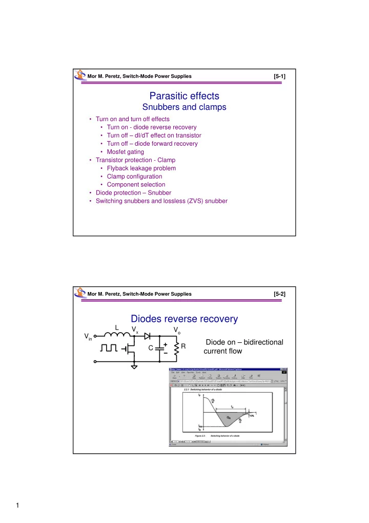
Parasitic effects
Snubbers and clamps
- Turn on and turn off effects
- Turn on - diode reverse recovery
- Turn off – dI/dT effect on transistor
- Turn off – diode forward recovery
- Mosfet gating
- Transistor protection - Clamp
- Flyback leakage problem
- Clamp configuration
- Component selection
- Diode protection – Snubber
- Switching snubbers and lossless (ZVS) snubber
Mor M. Peretz, Switch-Mode Power Supplies