
SLIDE 1
1
- Prof. S. Ben-Yaakov , DC-DC Converters
[6- 1]
Output Voltage Ripple, Parasitic Effects
6.1 Output voltage ripple (Buck) 6.2 Parasitic effects 6.2.1 Diode recovery 6.2.2 Internal delay of switching 6.2.3 Stray and leakage inductances
- Clamp
- Diode snubber (clamp)
- Switch snubbers
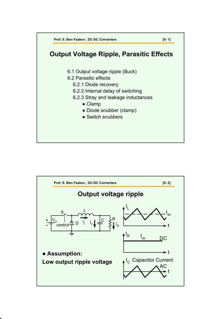
- Prof. S. Ben-Yaakov , DC-DC Converters
[6- 2]