
SLIDE 1
Digital Systems Connectors I CMPE 650 1 (5/3/07)
UMBC
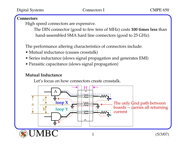
U M B C U N I V E R S I T Y O F M A R Y L A N D B A L T I M O R E C O U N T Y 1 9 6 6Connectors High speed connectors are expensive. The DIN connector (good to few tens of MHz) costs 100 times less than hand-assembled SMA hard line connectors (good to 25 GHz). The performance altering characteristics of connectors include:
- Mutual inductance (causes crosstalk)
- Series inductance (slows signal propagation and generates EMI)
- Parasitic capacitance (slows signal propagation)
Mutual Inductance Let’s focus on how connectors create crosstalk. H a c b The only Gnd path between boards -- carries all returning current loop X loop Y A