Microprocessors & Interfacing Concepts Standards USART in - - PowerPoint PPT Presentation

microprocessors interfacing
SMART_READER_LITE
LIVE PREVIEW

Microprocessors & Interfacing Concepts Standards USART in - - PowerPoint PPT Presentation

Lecture Overview Serial Communication Microprocessors & Interfacing Concepts Standards USART in AVR Serial Input/Output Lecturer : Dr. Annie Guo S2, 2008 COMP9032 Week10 1 S2, 2008 COMP9032 Week10 2 Serial


slide-1
SLIDE 1

S2, 2008 COMP9032 Week10 1

Microprocessors & Interfacing

Serial Input/Output

Lecturer : Dr. Annie Guo

S2, 2008 COMP9032 Week10 2

Lecture Overview

  • Serial Communication

– Concepts – Standards

  • USART in AVR

S2, 2008 COMP9032 Week10 3

Why Serial I/O?

  • Problems with Parallel I/O:

– Needs a wire for each bit. – When the source and destination are more than a few feet the parallel cable can be bulky and expensive. – Susceptible to reflections and induced noises for long distance communication.

  • Serial I/O overcomes these problems.

S2, 2008 COMP9032 Week10 4

Transmit Data Buffer Parallel In/Serial Out Shift Register Data From Source Received Data Buffer Serial In/Parallel Out Shift Register Data To Destination Serial Data Tclock Rclock TRANSMITTER RECEIVER n n

Serial Communication System Structure

slide-2
SLIDE 2

S2, 2008 COMP9032 Week10 5

Serial Communication System Structure (cont.)

  • At the communication source:

– The parallel interface transfers data from the source to the transmit data buffer. – The data is loaded into the Parallel In Serial Out (PISO) register and Tclock shifts the data bits out from the shift register to the receiver.

S2, 2008 COMP9032 Week10 6

Serial Communication System Structure (cont.)

  • At the communication destination:

– Rclock shifts each bit received into the Serial In Parallel Out (SIPO) register. – After all data bits have been shifted in, they are transferred to the received data buffer. – The data in the received data buffer can be read by an input operation via the parallel interface.

S2, 2008 COMP9032 Week10 7

Serial Communication

  • There are two basic types of serial

communications

– synchronous – asynchronous

S2, 2008 COMP9032 Week10 8

Synchronous VS Asynchronous

  • Synchronous

– Transmitter and receiver are synchronized

  • Need extra hardware for clock synchronization

– Having faster data transfer rate

  • Asynchronous

– Transmitter and receiver use different clocks. No clock synchronization is required. – Used in many applications such as keyboards, mice, modems – The rest of this lecture focuses on Asynchronous communication

slide-3
SLIDE 3

S2, 2008 COMP9032 Week10 9

UART

  • The device that implements both transmitter and

receiver in a single integrated circuit is called a UART (Universal Asynchronous Receiver/Transmitter).

  • UART uses least significant first order

– The least significant bit of data is transferred first

  • Data are transmitted asynchronously.

– Clocks on both sides are not synchronized – But receivers have a way to synchronise the data receiving

  • peration with data transmission operation
  • UART is the basis for most serial communication

hardware.

S2, 2008 COMP9032 Week10 10

UART Structure

Transmitter Receiver UART Receiver Transmitter UART Tclock1 Rclock1 Tclock2 Rclock2 Data Bus

Data Bus

S2, 2008 COMP9032 Week10 11

UART Data Formats

  • Before transmission, data should be encoded

– Many encoding schemes, such as ASCII

  • Each encoded data is encapsulated with two bits

– Start bit and stop bit

  • Mark and space: the logic one and zero levels are

called mark and space.

– When the transmitter is not sending anything, it holds the line at mark level, also called idle level. Least Significant Bit Optional Parity Bit Stop Bit Start Bit Data Bits Mark Space

S2, 2008 COMP9032 Week10 12

UART Data Formats (cont.)

  • Typical bits in data transmission:

– Start bit: When the transmitter has data to send, it first changes the line from the mark to the space level for one bit

  • time. This synchronises the receiver with transmitter. When

the receiver detects the start bit, it knows to start clocking in the serial data bits. – Data bits: representing a data, such as a character – Parity bit: used to detect errors in the data

  • For odd parity: the bit makes the total number of 1s in the data
  • dd
  • For even parity: the bit makes the total number of 1s in the data

even.

– Stop bit: added at the end of data bits. It gives one bit-time between successive data. Some systems require more than

  • ne stop bit.
slide-4
SLIDE 4

S2, 2008 COMP9032 Week10 13

Data Transmission Rate

  • The rate at which bits are transmitted is called

baud rate.

  • It is given in bits per second
  • Standard data rates – Baud:

110, 150, 300, 600, 900, 1200, 2400, 4800, 9600, 14400, 19200, 38400, 57800

S2, 2008 COMP9032 Week10 14

Communication System Types

  • Three ways that data can be sent in serial

communication system:

– Simplex system – Full-duplex (FDX) system – Half-duplex (HDX) system

S2, 2008 COMP9032 Week10 15

Simplex System

– Data are sent in one direction only

  • For example, computer to a serial printer.

– Simple

  • If the computer does not send data faster than the printer

can accept it, no handshaking signals are required.

– Two signal wires are needed for this system.

Computer Printer

S2, 2008 COMP9032 Week10 16

Full-Duplex (FDX) System

– Data are transmitted in two directions. – It is called four-wire system, although only two signal wires and a common ground are sufficient.

Terminal Computer

slide-5
SLIDE 5

S2, 2008 COMP9032 Week10 17

Half-Duplex (HDX) System

– Data are transmitted in two directions with only

  • ne pair of signal lines.

– Additional hardware and handshaking signals must be added to an HDX system.

Computer Computer

S2, 2008 COMP9032 Week10 18

Standards for the Serial I/O Interface

  • Interface standards are needed to allow

different manufacturers’ equipment to be interconnected

  • Must define the following elements:

– Handshaking signals – Direction of data flow – Types of communication devices. – Connectors and interface mechanical considerations. – Electrical signal levels.

S2, 2008 COMP9032 Week10 19

Standards for the Serial I/O Interface (cont.)

  • Popular standards include RS-232-C, RS-

422, RS-423 and RS-485.

– RS-232-C standard is used in most serial interface. – If the signals must be transmitted farther than 50 feet or greater than 20 Kbits/second, another electrical interface standard such as RS-422, RS- 423 or RS-485 should be chosen. – For RS-422, RS-423 and RS-485, handshaking, direction of signal flow, and the types of communication devices are based on the RS-232- C standard.

S2, 2008 COMP9032 Week10 20

Two RS232-C Connectors

DE9 pin assignments DB25 pin assignments

slide-6
SLIDE 6

S2, 2008 COMP9032 Week10 21

DE9 DB25 Signal Purpose 1 PG Protective ground: this is actually the shield in a shielded cable. It is designed to be connected to the equipment frame and may be connected to external grounds. 3 2 TxD Transmitted data: Sourced by DTE and received by DCE. Data terminal equipment cannot send unless RTS, CTS, DSR and DTR are asserted. 2 3 RxD Received data: Received by DTE, sourced by DCE. 7 4 RTS Request to send: Sourced by DTE, received by DCE. RTS is asserted by the DTE when it wants to send data. The DCE responds by asserting CTS.

RS-232-C Signal Definitions

S2, 2008 COMP9032 Week10 22

DE9 DB25 Signal Purpose 8 5 CTS Clear to send: Sourced by DCE, received by DTE. CTS must be asserted before the DTE can transmit data. 6 6 DSR Data set ready: Sourced by DCE and received by DTE. Indicates that the DCE has made a connection on the telephone line and is ready to receive data from the

  • terminal. The DTE must see this asserted

before it can transmit data. 5 7 SG Signal ground: Ground reference for this signal is separate from pin 1, protective ground.

RS-232-C Signal Definitions (cont.)

S2, 2008 COMP9032 Week10 23

DE9 DB25 Signal Purpose 1 8 DCD Data carrier detect: Sourced by DCE, received by DTE. Indicates that a DCE has detected the carrier on the telephone line. Originally it was used in half-duplex systems but can be used in full-duplex systems, too. 4 20 DTR 9 22 RI Ring indicator: Sourced by DCE and received by DTE. Indicates that a ringing signal is detected. Data terminal ready: Sourced by DTE and received by DCE. Indicates that DTE is ready to send or receive data.

RS-232-C Signal Definitions (cont.)

S2, 2008 COMP9032 Week10 24

RS-232-C Interconnections

  • When two serial ports are connected, the data rate,

the number of data bits, whether parity is used, the type of parity, and the number of stop bits must be set properly and identically on each UART.

  • Proper cables must be used. There are four kinds of

cables from which to choose, depending on the types

  • f devices to be interconnected.

– Full DTE – DCE cable – Minimal DTE – DCE cable – DTE – DTE null modem cable – Minimal null modem cable

slide-7
SLIDE 7

S2, 2008 COMP9032 Week10 25

TxD 3 2 2 3 TxD RxD 2 3 3 2 RxD SG 5 7 7 5 SG RTS 7 4 4 7 RTS CTS 8 5 5 8 CTS DCD 1 8 8 1 DCD DSR 6 6 6 6 DSR DTR 4 20 20 4 DTR DTE DTE DCE DCE DE9 DB25 DB25 DE9 Full DTE – DCE cable

RS-232-C Interconnections (cont.)

S2, 2008 COMP9032 Week10 26

TxD 3 2 2 3 TxD RxD 2 3 3 2 RxD SG 5 7 7 5 SG RTS 7 4 4 7 RTS CTS 8 5 5 8 CTS DCD 1 8 8 1 DCD DSR 6 6 6 6 DSR DTR 4 20 20 4 DTR DTE DTE DCE DCE DE9 DB25 DB25 DE9 Minimal DTE-DCE cable

RS-232-C Interconnections (cont.)

S2, 2008 COMP9032 Week10 27

TxD 3 2 2 3 TxD RxD 2 3 3 2 RxD SG 5 7 7 5 SG RTS 7 4 4 7 RTS CTS 8 5 5 8 CTS DCD 1 8 8 1 DCD DSR 6 6 6 6 DSR DTR 4 20 20 4 DTR DTE DTE DTE DTE DE9 DB25 DB25 DE9 DTE – DTE null modem cable

RS-232-C Interconnections (cont.)

S2, 2008 COMP9032 Week10 28

TxD 3 2 2 3 TxD RxD 2 3 3 2 RxD SG 5 7 7 5 SG RTS 7 4 4 7 RTS CTS 8 5 5 8 CTS DCD 1 8 8 1 DCD DSR 6 6 6 6 DSR DTR 4 20 20 4 DTR DTE DTE DTE DTE DE9 DB25 DB25 DE9 Minimal null modem cable

RS-232-C Interconnections (cont.)

slide-8
SLIDE 8

S2, 2008 COMP9032 Week10 29

RS-232-C Logic levels: Mark -25 to –3 volts Space +25 to +3 volts

D R RS-232-C Logic levels TTL Logic levels TTL Logic levels

RS-232-C Interface

S2, 2008 COMP9032 Week10 30

RS-423 Standard

  • Also a single ended system.
  • Allows longer distance and higher data rates than

RS-232-C.

  • Allows a driver to broadcast data to 10 receivers.

D R R Up to 10 receivers RS-423 Interface

S2, 2008 COMP9032 Week10 31

RS-422 Standard

  • RS-422 line drivers and receivers operates

with differential amplifier.

– These drivers eliminate much of the common- mode noise experienced with long transmission lines, thus allowing the longer distances and higher data rates.

D R R Up to 10 receivers RS-422 Interface

S2, 2008 COMP9032 Week10 32

RS-485 Standard

  • Similar to RS-422 in that it uses differential line

drivers and receivers.

  • Unlike RS-422, RS-485 provides for multiple drivers

and receivers in a bussed environment.

– Up to 32 drivers/receivers pairs can be used together. D R R Up to 32 receivers RS-485 Interface D Up to 32 drivers

slide-9
SLIDE 9

S2, 2008 COMP9032 Week10 33

Specification RS-232-C RS-423 RS-422 RS-485 Receiver input ±3 to ±15V ±200mV to ±12V ±200mV to ±200mV to voltage ±7V -7 to +12V Driver output signal ±5 to ±15V ±3.6 to ±6V ±2 to ±5V ±1.5 to ±5V Maximum data rate 20 Kb/s 100 Kb/s 10 Mb/s 10 Mb/s Maximum cable 50 ft 4000 ft 4000 ft 4000 ft length Driver source 3-7 KΩ 450 Ω min 100 Ω 54Ω Impedance Receiver input 3 KΩ 4 KΩ min 4 K Ω min 12 KΩ minimum resistance Mode Singled-ended Singled-ended Differential Differential Number of drivers 1 Driver 1 driver 1 Driver 32 Driver and receivers allowed on one line 1 Receivers 10 Receivers 10 Receivers 32 Receivers

Summary of Standards

S2, 2008 COMP9032 Week10 34

AVR USARTs

  • Two USART units

– Unit 0 – Unit 1

  • Each unit can be configured for synchronous
  • r asynchronous serial communication
  • USART unit 0 is used on our lab board to

receive program code downloaded from the PC host via USB

S2, 2008 COMP9032 Week10 35

AVR USARTs (cont.)

  • Support many serial frames.
  • Have transmission error detection

– Odd or even parity error – Framing error

  • Three interrupts on

– TX Complete – TX Data Register Empty – RX Complete.

S2, 2008 COMP9032 Week10 36

USART Block Diagram

slide-10
SLIDE 10

S2, 2008 COMP9032 Week10 37

AVR USART Structure

  • The USART consists of three components:

clock generator, transmitter and receiver

  • Clock generator

– consists of synchronization logic for external clock input used by synchronous slave operation, and the baud rate generator.

  • Transmitter

– consists of a single write buffer, a serial Shift Register, Parity Generator and Control Logic for handling different serial frame formats.

S2, 2008 COMP9032 Week10 38

AVR USART Structure (cont.)

  • Receiver

– The Receiver is the most complex part of the USART module due to its clock and data recovery units.

  • The recovery units are used for asynchronous data

reception.

– In addition to the recovery units, the Receiver includes a Parity Checker, Control Logic, a Shift Register and a Receive Buffer (UDR). – The Receiver supports the same frame formats as the Transmitter, and can detect Frame Error, Data Over Run and Parity Error.

S2, 2008 COMP9032 Week10 39

Frame Formats

  • Up to 30 formats

– combinations of

  • 1 start bit (St)
  • 5, 6, 7, 8, or 9 data bits
  • no, even or odd parity bit (P)
  • 1 or 2 stop bits (Sp)
  • Example

S2, 2008 COMP9032 Week10 40

Parity Bit

  • Used to check whether the received data is

different from the sending data

  • Two forms of the parity bit

– Even parity – Odd parity – Where di in the two formulas is a data bit, n is the number of data bits.

d d d d P

1 1 n n even

⊕ ⊕ ⊕ ⊕ ⊕ ⊕ ⊕ ⊕ ⊕ ⊕ ⊕ ⊕ ⋅ ⋅ ⋅ ⋅ ⋅ ⋅ ⋅ ⋅ ⋅ ⋅ ⋅ ⋅ ⊕ ⊕ ⊕ ⊕ ⊕ ⊕ ⊕ ⊕ = = = =

− − − −

1 d d d d P

1 1 n n

  • dd

⊕ ⊕ ⊕ ⊕ ⊕ ⊕ ⊕ ⊕ ⊕ ⊕ ⊕ ⊕ ⋅ ⋅ ⋅ ⋅ ⋅ ⋅ ⋅ ⋅ ⋅ ⋅ ⋅ ⋅ ⊕ ⊕ ⊕ ⊕ ⊕ ⊕ ⊕ ⊕ = = = =

− − − −

slide-11
SLIDE 11

S2, 2008 COMP9032 Week10 41

Control Registers

  • Three control registers are used in USART
  • peration:

– UCSRA

  • for storing the status flags of USART
  • for controlling transmission speed and use of multiple

processors

– UCSRB

  • for enabling interrupts, transmission operations
  • for setting frame formats
  • for bit extension

– UCSRC

  • For operation configuration

S2, 2008 COMP9032 Week10 42

UCSRA

  • USART Control and Status Register A

S2, 2008 COMP9032 Week10 43

UCSRA Bit Descriptions

  • Bit 7 – RXC: USART Receive Complete

– Set when the receive buffer is not empty – The RXC flag can be used to generate a Receive Complete interrupt

  • Bit 6 – TXC: USART Transmit Complete

– Set when the entire frame in the Transmit Shift Register has been shifted out and there are no new data present in the transmit butter – TXC is automatically cleared when a transmit complete interrupt is executed. – TXC can generate a Transmit Complete interrupt

S2, 2008 COMP9032 Week10 44

UCSRA Bit Descriptions (cont.)

  • Bit 5 – UDRE: USART Data Register Empty

– Set when the transmit buffer (UDR) is empty – Can be used to generate a Data Register Empty interrupt

  • Bit 4 – FE: Frame Error

– Set when the next character in the receive buffer had a Frame Error when received.

  • Bit 3 – DOR: Data OverRun

– Set when a Data OverRun condition is detected. – A Data OverRun occurs when the receive buffers are all full and a new start bit is detected.

slide-12
SLIDE 12

S2, 2008 COMP9032 Week10 45

UCSRA Bit Descriptions (cont.)

  • Bit 2 – UPE: USART Parity Error

– Set when the next character in the receive buffer had a Parity Error when received and the Parity Checking was enabled

  • Bit 1 – U2X: Double the USART Transmission Speed

– Set for doubling the transfer rate for asynchronous communication

  • Bit 0 – MPCM: Multi-processor Communication Mode

– If set, all the incoming frames received by the USART Receiver that do not contain address information will be ignored.

S2, 2008 COMP9032 Week10 46

UCSRB

  • USART Control and Status Register B

S2, 2008 COMP9032 Week10 47

UCSRB Bit Descriptions

  • Bit 7 – RXCIE: RX Complete Interrupt Enable

– Set to enable interrupt on the RXC flag

  • Bit 6 – TXCIE: TX Complete Interrupt Enable

– Set to enable interrupt on the TXC flag

  • Bit 5 – UDRIE: USART Data Register Empty

Interrupt Enable

– Set to enable interrupt on the UDRE flag.

S2, 2008 COMP9032 Week10 48

UCSRB Bit Descriptions (cont.)

  • Bit 4 – RXEN: Receiver Enable

– Set the enable the USART receiver. – The Receiver will override normal port operation for the RxD pin when enabled. Disable the Receiver will flush the receive buffer invalidating the FE, DOR and UPE flags.

  • Bit 3 – TXEN: Transmitter Enable

– Set to enable the USART Transmitter – The Transmitter will override normal port

  • perations for the TxD pin when enabled. The

disabling of the Transmitter will not become effective until transmissions are complete.

slide-13
SLIDE 13

S2, 2008 COMP9032 Week10 49

UCSRB Bit Descriptions (cont.)

  • Bit 2 – UCSZ2: Character Size

– The bit combined with the UCSZ1:0 bits in UCSRC sets the number of data bits in a frame.

  • Bit 1 – RXB8: Receive Data Bit 8

– The ninth data bit of the received character when operating with serial frames with nine data bits. Must be read before reading the low bits from UDR

  • Bit 0 – TXB8: Transmit Data Bit 8

– The ninth data bit in the character to be transmitted when

  • perating with serial frames with nine data bits. Must be

written before writing the low bits to UDR

S2, 2008 COMP9032 Week10 50

UCSRC

  • USART Control and Status Register C

S2, 2008 COMP9032 Week10 51

UCSRC Bit Descriptions

  • Bit 6 – UMSEL: USART Mode Select

– 0: Asynchronous Operation – 1: Synchronous Operation

  • Bit 5:4 – UPM1:0: Parity Mode

– Set to enable Parity bit operation UPM1 UPM0 Parity Mode Disabled 1 Reserved 1 Enabled, Even Parity 1 1 Enabled, Odd Parity

S2, 2008 COMP9032 Week10 52

UCSRC Bit Descriptions (cont.)

  • Bit 3 – USBS: Stop Bit Select

– 0: 1-bit – 1: 2-bit

  • Bit 2:1 – UCSZ1:0: Character Size

– Together with UCSZ2 to determine the number of bits for a character

UCSZ2 UCSZ1 UCSZ0 Character Size 5-bit 1 6-bit 1 7-bit 1 1 8-bit 1 Reserved 1 1 Reserved 1 1 Reserved 1 1 1 9-bit

slide-14
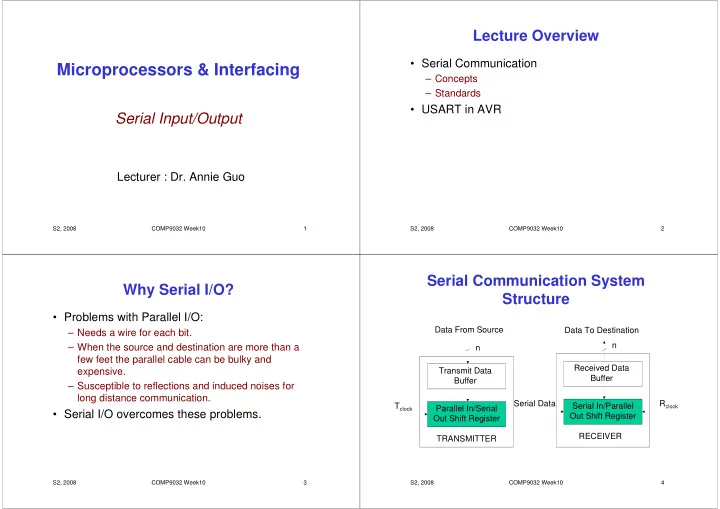
SLIDE 14

S2, 2008 COMP9032 Week10 53

UCSRC Bit Descriptions (cont.)

  • Bit 0 – UCPOL: Clock Polarity

UCPOL Transmitted Data Changed Received Data Sampled (Output of TxD Pin) (Input on RxD Pin) Rising XCK Edge Failing XCK Edge 1 Failing XCK Edge Rising XCK Edge

S2, 2008 COMP9032 Week10 54

USART Initialization

  • Initialization process consists of

– Setting the baud rate, – Setting the frame format; and – Enabling the Transmitter or the Receiver

  • For interrupt driven USART operation, the

Global Interrupt Flag should be cleared when doing the initialization

S2, 2008 COMP9032 Week10 55

Sample Code

  • Initialize USART 1

USART_Init: ; Set baud rate, which is stored in r17:r16 sts UBRR1H, r17 sts UBRR1L, r16 ; Enable receiver and transmitter ldi r16, (1<<RXEN1)|(1<<TXEN1) sts UCSR1B,r16 ; Set frame format: 8 bit data, 2 stop bits ldi r16, (1<<USBS1)|(3<<UCSZ10) sts UCSR1C,r16

S2, 2008 COMP9032 Week10 56

Data Transmission

  • The USART Transmitter is enabled by setting

the Transmit Enable (TXEN) bit in the UCSRB Register.

– A data transmission is initiated by loading the transmit buffer with the data to be transmitted.

  • The CPU can load the transmit buffer by writing to the

UDR I/O location. The buffered data in the transmit buffer will be moved to the Shift Register when the Shift Register is ready to send a new frame.

– The Shift Register is loaded with new data if it is in idle state (no ongoing transmission) or immediately after the last stop bit of the previous frame is transmitted. When the Shift Register is loaded with new data, it will transfer one complete frame at the rate given by the baud register, U2X bit or by XCK depending on mode of operation.

slide-15
SLIDE 15

S2, 2008 COMP9032 Week10 57

Sample code

  • Data Transmission

– The code below uses polling of the Data Register Empty (UDRE) flag.

  • When using frames with less than eight bits, the most

significant bits written to the UDR are ignored. USART_Transmit: ; Wait for empty transmit buffer lds r15, UCSR1A sbrs r15,UDRE1 rjmp USART_Transmit ; Put data (r16) into buffer, sends the data sts UDR1,r16

S2, 2008 COMP9032 Week10 58

Status of Data Transmission

  • The USART Transmitter has two flags that indicate

its state:

– USART Data Register Empty (UDRE)

  • Set: when the transmit buffer is empty and ready to receiver

new data

  • Clear: when the transmit butter contains data to be moved into

the shift register

– Transmit Complete (TXC)

  • Set: when data in the Transmit Shift Register has been shifted
  • ut and there are no new data currently present in the transmit

buffer

  • Clear: otherwise
  • Both flags can be used for generating interrupts.

S2, 2008 COMP9032 Week10 59

Data Reception

  • The USART Receiver is enabled by writing

the Receive Enable (RXEN) bit in the UCSRB Register

– The baud rate, mode of operation and frame format must be set up once before doing any

  • transmissions. If synchronous operation is used,

the clock on the XCK pin will be overridden and used as transmission clock.

S2, 2008 COMP9032 Week10 60

Sample code

  • Data reception

USART_Receive: ; Wait for data to be received lds r10, UCSR1A sbrs r10, RXC1 rjmp USART_Receive ; Get and return received data from buffer lds r16, UDR1

slide-16
SLIDE 16

S2, 2008 COMP9032 Week10 61

Status of Data Reception

  • The Receive Complete (RXC) flag indicates if

there are unread data present in the receive buffer.

– Set: when unread data exist in the receive buffer – Clear: otherwise

  • If the receiver is disabled (RXEN = 0), the

receive buffer will be flushed and consequently the RXC bit will become zero.

S2, 2008 COMP9032 Week10 62

Error Detection

  • Three errors are checked on the receiver

side:

– Frame error

  • By checking whether the first stop bit is corrected

received

– Parity error

  • By checking whether the data received has the same

(odd or even) number of 1’s as in the data from the tranmistter.

– Data OveRun error

  • By checking if any data is yet read but is overwritten by

incoming data frame.

S2, 2008 COMP9032 Week10 63

Error Recovery

  • Main sources of errors in asynchronous data

transmission

– Data reception is “out sync” with transmission – Noise added to the data

S2, 2008 COMP9032 Week10 64

Error Recovery (cont.)

  • AVR includes a clock recovery and a data

recovery unit for handling errors in asynchronous transmission.

– The clock recovery logic is used for synchronizing the internally generated baud rate clock to the incoming asynchronous serial frames at the RxD pin.

  • Based on the start bit

– The data recovery logic samples and low pass filters each incoming bit, thereby improving the noise immunity of the Receiver

  • Based on multiple sampling and majority policy for each

incoming bit

slide-17
SLIDE 17

S2, 2008 COMP9032 Week10 65

Error Recovery (cont.)

  • The following figure gives an illustration

– The sample rate is 16 times the baud rate – When the Clock Recovery logic detects a high (idle) to low (start) transition on the RxD line, it uses the samples 8, 9 and 10 to decide if it is a valid bit (namely, 0)

  • If the majority of the three bits are 0, the bit is valid; data

recovery is followed.

  • If the majority of the three bits are 1, the bit is invalid; the

circuit looks for next start bit.

S2, 2008 COMP9032 Week10 66

Error Recovery (cont.)

– When the receiver clock is synchronized to the start bit, the data recovery can begin for each subsequent data bit. – The decision of the logic level of the received bit is taken by doing a majority voting of the logic value to the three samples in the center of the received bit.

S2, 2008 COMP9032 Week10 67

Reading Material

  • Chapter 10: Serial Input/Output.

Microcontrollers and Microcomputers by Fredrick M. Cady.

  • Mega64 Data Sheet

– USART