microprocessors interfacing
play

Microprocessors & Interfacing Input switches Basics of - PowerPoint PPT Presentation

Lecture Overview Input devices Microprocessors & Interfacing Input switches Basics of switches Keypads Input/Output Devices Output devices LCD Lecturer : Dr. Annie Guo S2, 2008 COMP9032 Week8 1 S2, 2008


  1. Lecture Overview • Input devices Microprocessors & Interfacing – Input switches • Basics of switches – Keypads Input/Output Devices • Output devices – LCD Lecturer : Dr. Annie Guo S2, 2008 COMP9032 Week8 1 S2, 2008 COMP9032 Week8 2 Input Switches Input Switches (cont.) • Most basic binary input devices Vcc • The switch output is high or low, depending Vcc on the switch position. R Typically 1K Ohm • Pull-up resistors are necessary in each switch Logic high with switch open to provide a high logic level when the switch Logic low with switch closed ½ is open. Data Bus 74LS244 Octal • Problem with switches: Buffer – Switch bounce. • When a switch makes contact, its mechanical (a) Single-pole, single-throw (b) Multiple pole switch. springiness will cause the contact to bounce, or contact (SPST) logic switch Data and break, for a few milliseconds (typically 5 to 10 ms). Bus S2, 2008 COMP9032 Week8 3 S2, 2008 COMP9032 Week8 4
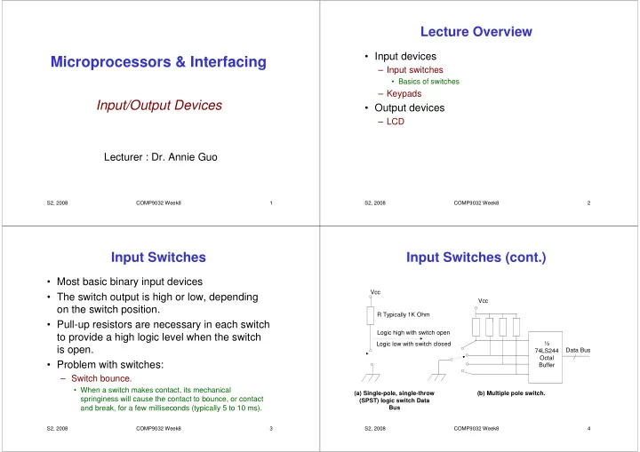
  2. NAND Latch Debouncer Software Debouncing • Basic idea: wait until the switch is stable • For example: Vcc – Wait and see: • If the software detects a low logic level, indicating that switch has closed, it simply waits for some time, say 20 to 100ms, and then test if the switch is still low. Logic high with switch up – Counter-based approach: • Initialize a counter to 10. Logic low with switch down • Poll the switch every millisecond until the counter is either 0 or 20. If the switch output is low, decrease the counter; otherwise, increment the counter. • If the counter is 0, we know that switch output has been low (closed) for at least 10 ms. If, on the other hand, the counter reaches 20, we know that the switch has been open for at least 10 ms. S2, 2008 COMP9032 Week8 5 S2, 2008 COMP9032 Week8 6 One-Dimensional Array of One-Dimensional Array of Switches Switches Vcc A • Switch bouncing problem must be solved – Either using software or hardware • The array of switches must be scanned to I0 74LS151 8 to 1 find out which switches are closed or open. I1 Multiplexer Scanned Switch Data I2 – Software is required to scan the array. As the I3 To Input Port software outputs a 3-bit sequence from 000 to Z I4 111, the multiplexer selects each of the switch I5 inputs. I6 I7 – The output of switch array could be interfaced E S2 S1 S0 directly to an eight-bit port at point A. Selected Input From Output Port S2, 2008 COMP9032 Week8 7 S2, 2008 COMP9032 Week8 8

  3. Keyboard Matrix of Switches Keyboard Matrix of Switches Vcc (cont.) 12 74LS151 8-to-1 A • A keyboard is an array of switches arranged Input Multiplexer in a two-dimensional matrix. I0 00 01 02 06 07 I1 • A switch is connected at each intersection of 10 11 12 17 I2 Scanned Switch vertical and horizontal lines. Data I3 To Input Port Z • Closing the switch connects the horizontal I4 line to the vertical line. I5 I6 • 8*8 keyboard can be interfaced directly into I7 B 70 71 77 8-bit output and input ports at point A and B. E S2 S1 S0 Vcc O0 O1 O2 O3 O4 O5 O6 O7 E3 E2 E1 A2 A1 A0 Select Input From Output Port 74LS138 3-of-8 Decoder Scan Input From Output Port S2, 2008 COMP9032 Week8 9 S2, 2008 COMP9032 Week8 10 Keyboard Matrix of Switches Ghosting (cont.) • Software can scan the key board by Vcc outputting a three-bit code to the decoder and then scanning the multiplexer to find the closed switch or switches. R3 R2 R1 Col 0 Col 1 Col 2 – The combination of the two 3-bit scan codes 00 01 02 Row 0 (Pulled low, error) (A2A1A0 and S2S1S0) identifies which switch is 10 11 12 Row 1 (Pulled low, OK) closed. For example, the code 000000 scan 20 21 22 switch 00 in the upper left-hand corner. Row 2 (High, OK) • The diode prevents a problem called Low ghosting. (Scanned column) S2, 2008 COMP9032 Week8 11 S2, 2008 COMP9032 Week8 12

  4. Ghosting (cont.) Example • Ghosting occurs when several keys are pushed at • Get an input from 4*4 keypad once. • Consider the case shown in the figure where three switches 01, 10 and 11 are all closed. Column 0 is selected with a logic low and assume that the circuit does not contain the diodes. As the rows are scanned, a low is sensed on Row 1, which is 1 A 2 3 R0 acceptable because switch 10 is closed. In addition, 4 5 6 B R1 Row 0 is seen to be low, indicating switch 00 is 7 8 C R2 9 closed, which is NOT true. The diodes in the switches 0 # D R3 * eliminate this problem by preventing current flow from C0 C1 C2 C3 R1 through switches 01 and 11. Thus Row 0 will not be low when it is scanned. S2, 2008 COMP9032 Week8 13 S2, 2008 COMP9032 Week8 14 Example (solution) Code Implementation • Algorithm ; The program gets input from keypad and displays its ascii value on the ; LED bar Scan columns from left to right .include "m64def.inc" for each column, scan rows from top to bottom .def row =r16 ; current row number for each key being scanned if it is pressed .def col =r17 ; current column number .def rmask =r18 ; mask for current row during scan display .def cmask =r19 ; mask for current column during scan wait endif .def temp1 =r20 .def temp2 =r21 endfor endfor Repeat the scan process .equ PORTDDIR =0xF0 ; PD7-4: output, PD3-0, input .equ INITCOLMASK = 0xEF ; scan from the leftmost column, – A column is selected, its related Cx value is set to 0. .equ INITROWMASK = 0x01 ; scan from the top row .equ ROWMASK =0x0F ; for obtaining input from Port D – A mask is used to read one row at a time. S2, 2008 COMP9032 Week8 15 S2, 2008 COMP9032 Week8 16

  5. Code Implementation Code Implementation colloop: RESET: cpi col, 4 ;ldi temp1, low(RAMEND) ; initialize the stack breq main ; if all keys are scanned, repeat ;out SPL, temp1 out PORTD, cmask ; otherwise, scan a column ;ldi temp1, high(RAMEND) ;out SPH, temp1 ldi temp1, 0xFF ; slow down the scan operation delay: dec temp1 ldi temp1, PORTDDIR ; PD7:4/PD3:0, out/in brne delay out DDRD, temp1 ser temp1 ; PORTC is output in temp1, PIND ; read PORTD out DDRC, temp1 andi temp1, ROWMASK ; get the keypad output value out PORTC, temp1 cpi temp1, 0xF ; check if any row is low breq nextcol main: ; if yes, find which row is low ldi cmask, INITCOLMASK ; initial column mask ldi rmask, INITROWMASK ; initialize for row check clr col ; initial column clr row ; S2, 2008 COMP9032 Week8 17 S2, 2008 COMP9032 Week8 18 Code Implementation Code Implementation rowloop: convert: cpi row, 4 cpi col, 3 ; if the pressed key is in col.3 breq nextcol ; the row scan is over. breq letters ; we have a letter mov temp2, temp1 and temp2, rmask ; check un-masked bit ; if the key is not in col.3 and breq convert ; if bit is clear, the key is pressed inc row ; else move to the next row cpi row, 3 ; if the key is in row3, lsl rmask breq symbols ; we have a symbol or 0 jmp rowloop mov temp1, row ; otherwise we have a number in 1-9 nextcol: ; if row scan is over lsl temp1 lsl cmask add temp1, row ; inc col ; increase column value add temp1, col ; temp1 = row*3 + col jmp colloop ; go to the next column subi temp1, -'1' ; add the value of character ‘1’ jmp convert_end S2, 2008 COMP9032 Week8 19 S2, 2008 COMP9032 Week8 20

  6. Code Implementation LCD letters: • Liquid Crystal Display ldi temp1, 'A' add temp1, row ; Get the ASCII value for the key • Programmable output device jmp convert_end symbols: cpi col, 0 ; check if we have a star breq star cpi col, 1 ; or if we have zero breq zero ldi temp1, '#' ; if not we have hash jmp convert_end star: ldi temp1, '*' ; set to star jmp convert_end zero: ldi temp1, '0' ; set to zero convert_end: out PORTC, temp1 ; write value to PORTC jmp main ; restart main loop S2, 2008 COMP9032 Week8 21 S2, 2008 COMP9032 Week8 22 Dot Matrix LCD Pin Assignments • Characters are displayed using a dot matrix. – 5x7, 5x8, and 5x11 • A controller is used for communication between the LCD and other devices,e.g. MPU • The controller has an internal character generator ROM. All display functions are controllable by instructions. S2, 2008 COMP9032 Week8 23 S2, 2008 COMP9032 Week8 24

  7. Pin Descriptions Dot Matrix LCD Diagram S2, 2008 COMP9032 Week8 25 S2, 2008 COMP9032 Week8 26 Operations Operations (cont.) – The register select (RS) signal determines which • MPU communicates with LCD through two of these two register is selected. registers – Instruction Register (IR) • To store instruction code like Display clear or Cursor Shift as well as addresses for the Display Data RAM (DD RAM) or the Character Generator RAM (CG RAM) – Data Register (DR) • To temporarily store data to be read/written to/from the DD RAM of the display controller. S2, 2008 COMP9032 Week8 27 S2, 2008 COMP9032 Week8 28

Download Presentation
Download Policy: The content available on the website is offered to you 'AS IS' for your personal information and use only. It cannot be commercialized, licensed, or distributed on other websites without prior consent from the author. To download a presentation, simply click this link. If you encounter any difficulties during the download process, it's possible that the publisher has removed the file from their server.

Recommend


More recommend