lecture 25 surfaces scanning tunneling microscope
play

Lecture 25: Surfaces Scanning Tunneling Microscope Special - PowerPoint PPT Presentation

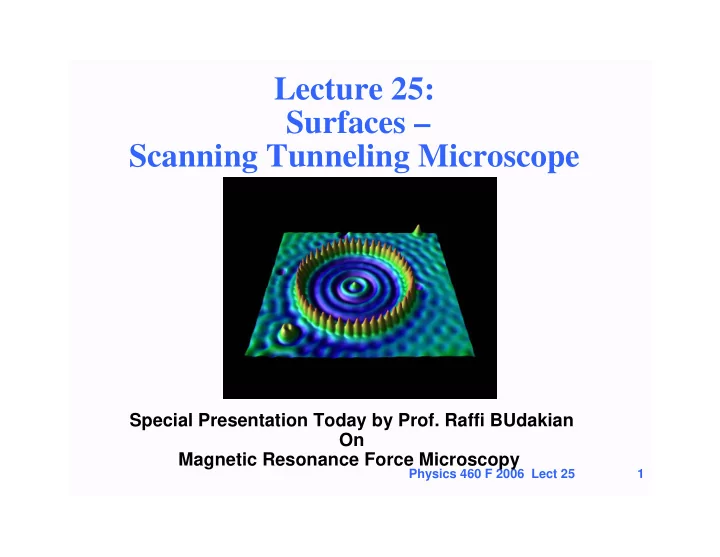
Lecture 25: Surfaces Scanning Tunneling Microscope Special Presentation Today by Prof. Raffi BUdakian On Magnetic Resonance Force Microscopy Physics 460 F 2006 Lect 25 1 Outline Surfaces of crystals Example surfaces of


  1. Lecture 25: Surfaces – Scanning Tunneling Microscope Special Presentation Today by Prof. Raffi BUdakian On Magnetic Resonance Force Microscopy Physics 460 F 2006 Lect 25 1

  2. Outline • Surfaces of crystals • Example – surfaces of semiconductors – GaAs • Tunneling in quantum mechanics Particles can tunnel through barriers • Scanning tunneling microscope -- STM • Examples of GaAs, Mn on GaAs, adatoms on Cu, atoms on GaN surface that illustrate growth, …. • AFM – very brief Physics 460 F 2006 Lect 25 2

  3. Surface structure – example: GaAs [110] Ga-As terminated (non-polar) [100] As terminated [100] Ga terminated Figure from Physics 460 F 2006 Lect 25 3 w3.rz-berlin.mpg.de/pc/ElecSpec/MBE/mbe.html

  4. Surface structure – example: GaAs (110) surface -Ga-As terminated Note the As atoms are slightly higher than the Ga atoms Conventional Cubic Cell in the bulk crystal Top view of (110) surface Note zig-zag chains of Ga and As atoms Figures from PhD thesis of Physics 460 F 2006 Lect 25 4 Dale Kitchen, U of Illinois, 2006

  5. “Seeing” atomic scale features “Scanning Tunneling Microscope” Measures electric current from tip to surface as tip is moved Probe manipulated by electric controls ---- very sharp tip Surface Feature on surface Physics 460 F 2006 Lect 25 5

  6. Scanning Tunneling Microscope Nobel Prize 1985 Tip Single atom at tip Extra atom on surface Electrons “Tunnel” Surface from tip to surface “reconstruction” Rate of tunneling extremely sensitive to distance of tip from surface due to quantum effects Physics 460 F 2006 Lect 25 6

  7. “Tunneling” in quantum mechanics • In Quantum Mechanics has a non-zero probability to be in region that is “classically forbidden” • A particle can tunnel through a barrier even though it does not have enough energy to get over the barrier A particle on the left Energy of particle has some probability 0 < E < V 0 V=V 0 to tunnel through the potential barrier to the Potential right side Energy V(x) Energy V=0 Position x Physics 460 F 2006 Lect 25 7

  8. Schrodinger Equation • Basic equation of Quantum Mechanics [ - (h 2 /2m)d 2 /dx 2 + V(x) ] Ψ (x) = E Ψ (x) where we consider only one dimension m = mass of particle V(x) = potential energy at point x ∆ E = eigenvalue = energy of quantum state Ψ (x) = wavefunction n (x) = | Ψ (x) | 2 = probability density •Key issue for tunneling: What happens if the energy E is less than the potential V at some point x Physics 460 F 2006 Lect 25 8

  9. Schrodinger Equation II • Consider the case where V = constant = V 0 [ - (h 2 /2m)(d 2 /dx 2 )+ V 0 ] Ψ (x) = E Ψ (x) which can be written (h 2 /2m) )(d 2 /dx 2 ) Ψ (x) = [V 0 - E ] Ψ (x) or (d 2 /dx 2 ) Ψ (x) = - k 2 Ψ (x), k 2 = (E - V 0 )(2m/h 2 ) •If E > V 0 , Ψ (x) ~ e -ikx (the same as before) • If E < V 0 , define κ 2 = - k 2 , Ψ (x) ~ e - κ x • The wavefuntion decays exponentially in the region where E < V Physics 460 F 2006 Lect 25 9

  10. “Tunneling” in quantum mechanics • In Quantum Mechanics has a non-zero probability to be in region that is “classically forbidden” • A particle can tunnel through a barrier even though it does not have enough energy to get over the barrier Energy of particle Probability of tunneling 0 < E < V 0 | A Richt | 2 Potential V=V 0 = Potential Energy V(x) Energy V(x) | A Left | 2 Ψ (x) = A Left e -ikx Ψ (x) = A Right e -ikx V=0 Position x Physics 460 F 2006 Lect 25 10

  11. Scanning Tunneling Microscope Tip Single atom at tip Extra atom on surface Electrons “Tunnel” Surface from tip to surface “reconstruction” Probability for an electron to “tunnel” from the metal tip to the surface varies rapidly with the distance Physics 460 F 2006 Lect 25 11

  12. STM images – example: GaAs (110) Surface (110) Surface model top view Image of As atoms Model showing Ga and As zig-zag chains Figures from PhD thesis of Physics 460 F 2006 Lect 25 12 Dale Kitchen, U of Illinois, 2006

  13. STM image - Mn atom on GaAs GaAs (110) Surface with one added Mn atom at position indicated by x Figures from PhD thesis of Physics 460 F 2006 Lect 25 13 Dale Kitchen, U of Illinois, 2006

  14. STM image – subsurface atoms Shape indicates the directions of the electron bonds Bonds to surface atoms Bonds to the other neighbors GaAs (110) surface with Zn, Mn, Fe or Co atoms substituted for Ga in the first layer below the surface Figures from PhD thesis of Physics 460 F 2006 Lect 25 14 Dale Kitchen, U of Illinois, 2006

  15. Observation of atoms, electron waves with Scanning Tunneling Microscope Physics 460 F 2006 Lect 25 15

  16. Observation of atoms, electron waves with Scanning Tunneling Microscope Corral of atoms placed one at the time by maneuvering atoms with STM Electron standing waves inside the “corral” Surface Atoms Extra atom Physics 460 F 2006 Lect 25 16 Figure by D. Eigler, et. al, IBM Research

  17. Surface of GaN observed by STM Atomic scale structure of Spiral growth -- surface A common way that crystals grow -- by adding atoms at a “Step” on surface step, the higher layer where the surface grows over the lower height changes layer – continues in a by one layer spiral Step Adding atoms at step makes step Side view move to cover lower layer Step Side view Figure by D. Smith, reproduced in Electronic Structure”, by R. M. Martin, Physics 460 F 2006 Lect 25 17 Cambridge University Press 2004

  18. Atomic Force Microscope Article in Physics Today, December, 2006 Works for insulators, …. Si (111) surface From http://www.physik.uni-augsburg.de/exp6/research/sxm/sxm_e.shtml Physics 460 F 2006 Lect 25 18

  19. Summary • Surfaces of crystals • Example – surfaces of semiconductors – GaAs • Tunneling in quantum mechanics Particles can tunnel through barriers Exponential decay where E < V • STM – electrons tunnel through space between tip and sample Leads to the extreme sensitivity of tunneling current to the distanceof tip to sample Dominated by a single atom on tip • Examples of GaAs, Mn on GaAs, adatoms on Cu, atoms on GaN surface that illustrate growth, …. • AFM – very brief Physics 460 F 2006 Lect 25 19

  20. Next Lecture • Nanostructures Magnetic, superconducting • Final lecture ---- Summary of course Physics 460 F 2006 Lect 25 20

Download Presentation
Download Policy: The content available on the website is offered to you 'AS IS' for your personal information and use only. It cannot be commercialized, licensed, or distributed on other websites without prior consent from the author. To download a presentation, simply click this link. If you encounter any difficulties during the download process, it's possible that the publisher has removed the file from their server.

Recommend


More recommend