
SLIDE 1
Physics 460 F 2006 Lect 19 1
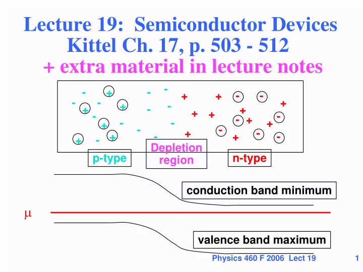
Lecture 19: Semiconductor Devices Kittel Ch. 17, p. 503 - 512 + extra material in lecture notes
p-type n-type +
- +
- +
+ + + +
- +
+ + + + + + +
- +
Lecture 19: Semiconductor Devices Kittel Ch. 17, p. 503 - 512 + - - PowerPoint PPT Presentation
Lecture 19: Semiconductor Devices Kittel Ch. 17, p. 503 - 512 + extra material in lecture notes - - + - + + - - - - + + - + - + + + - - - + - - + + - - + - + - + - + - Depletion p-type n-type region
Physics 460 F 2006 Lect 19 1
Physics 460 F 2006 Lect 19 2
Physics 460 F 2006 Lect 19 3
Physics 460 F 2006 Lect 19 4
Physics 460 F 2006 Lect 19 5
Physics 460 F 2006 Lect 19 6
Physics 460 F 2006 Lect 19 7
Physics 460 F 2006 Lect 19 8
Physics 460 F 2006 Lect 19 9
Physics 460 F 2006 Lect 19 10
Physics 460 F 2006 Lect 19 11
Physics 460 F 2006 Lect 19 12
Physics 460 F 2006 Lect 19 13
Physics 460 F 2006 Lect 19 14
Physics 460 F 2006 Lect 19 15
Physics 460 F 2006 Lect 19 16
Physics 460 F 2006 Lect 19 17
0 - ER 0 )
Physics 460 F 2006 Lect 19 18
0 - ER 0 - e(VL - VR) = ∆E0 - e∆V (with ∆V > 0)
Physics 460 F 2006 Lect 19 19
Physics 460 F 2006 Lect 19 20
Physics 460 F 2006 Lect 19 21
Physics 460 F 2006 Lect 19 22
Physics 460 F 2006 Lect 19 23
Physics 460 F 2006 Lect 19 24
Physics 460 F 2006 Lect 19 25
Physics 460 F 2006 Lect 19 26
Physics 460 F 2006 Lect 19 27
Physics 460 F 2006 Lect 19 28
Physics 460 F 2006 Lect 19 29
Physics 460 F 2006 Lect 19 30
Physics 460 F 2006 Lect 19 31
Physics 460 F 2006 Lect 19 32
Physics 460 F 2006 Lect 19 33
Physics 460 F 2006 Lect 19 34
Physics 460 F 2006 Lect 19 35
Physics 460 F 2006 Lect 19 36
valence band maximum conduction band minimum
valence band maximum conduction band minimum
Physics 460 F 2006 Lect 19 37
Physics 460 F 2006 Lect 19 38