
SLIDE 1
146
- 7. Semiconductor
- 7. Semiconductor
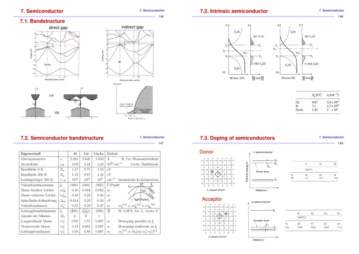
7.1. Bandstructure
direct gap indirect gap
147
7.2. Semiconductor bandstructure
- 7. Semiconductor
148
7.2. Intrinsic semiconductor
- 7. Semiconductor
149
7.3. Doping of semiconductors
- 7. Semiconductor