
SLIDE 1
Physics 460 F 2006 Lect 20 1
Lecture 20: Semiconductor Structures Kittel Ch 17, p 494-503, 507- - - PowerPoint PPT Presentation
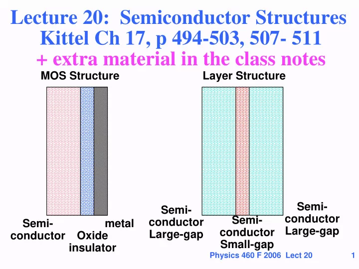
Lecture 20: Semiconductor Structures Kittel Ch 17, p 494-503, 507- 511 + extra material in the class notes MOS Structure Layer Structure Semi- Semi- conductor Semi- conductor Semi- metal Large-gap conductor Large-gap conductor Oxide
Physics 460 F 2006 Lect 20 1
Physics 460 F 2006 Lect 20 2
Physics 460 F 2006 Lect 20 3
Physics 460 F 2006 Lect 20 4
Physics 460 F 2006 Lect 20 5
Physics 460 F 2006 Lect 20 6
Physics 460 F 2006 Lect 20 7
Physics 460 F 2006 Lect 20 8
Physics 460 F 2006 Lect 20 9
Physics 460 F 2006 Lect 20 10
Physics 460 F 2006 Lect 20 11
Physics 460 F 2006 Lect 20 12
Physics 460 F 2006 Lect 20 13
Physics 460 F 2006 Lect 20 14
Physics 460 F 2006 Lect 20 15
Physics 460 F 2006 Lect 20 16
2 = (d2/dx2 + d2/dy2 + d2/dz2)
From Lecture 12 See Kittle, Ch 6
Physics 460 F 2006 Lect 20 17
L dx | Ψ (x) |2 = 1
From Lecture 12 See Kittle, Ch 6
Physics 460 F 2006 Lect 20 18
From Lecture 12 See Kittle, Ch 6
Physics 460 F 2006 Lect 20 19
From Lecture 12 See Kittle, Ch 6 In Lecture 12 we emphasized the limit that the box is very large
Physics 460 F 2006 Lect 20 20
2 , kz = n π/L, n = 1,2, ...
Here we emphasize the case where the box is very small
Physics 460 F 2006 Lect 20 21
2 + ky 2 + kz 2 )
2 + ky 2)
2 + ky 2)
Physics 460 F 2006 Lect 20 22
2 + ky 2)
Physics 460 F 2006 Lect 20 23
Physics 460 F 2006 Lect 20 24
Physics 460 F 2006 Lect 20 25
Physics 460 F 2006 Lect 20 26
Physics 460 F 2006 Lect 20 27
2 + ky 2)
Small-gap holes electrons L µ Layer of electrons at interface
Physics 460 F 2006 Lect 20 28
Physics 460 F 2006 Lect 20 29
Physics 460 F 2006 Lect 20 30
µ Layer of electrons at interface
Physics 460 F 2006 Lect 20 31
Physics 460 F 2006 Lect 20 32
Physics 460 F 2006 Lect 20 33
Physics 460 F 2006 Lect 20 34
Physics 460 F 2006 Lect 20 35
Physics 460 F 2006 Lect 20 36
Physics 460 F 2006 Lect 20 37
Physics 460 F 2006 Lect 20 38
Physics 460 F 2006 Lect 20 39
2 + ky 2 + kz 2 )
Physics 460 F 2006 Lect 20 40
2 , kz = n π/L, n = 1,2, ...
Physics 460 F 2006 Lect 20 41
2 + ky 2 + kz 2 ) = ( h2/2m ) k2