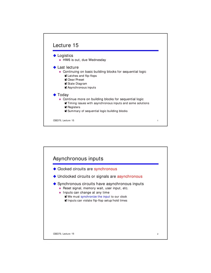
Lecture 15 Logistics HW6 is out, due Wednesday Last lecture - - PDF document

lecture 15
SMART_READER_LITE
LIVE PREVIEW

Lecture 15 Logistics HW6 is out, due Wednesday Last lecture - - PDF document

Lecture 15 Logistics HW6 is out, due Wednesday Last lecture Continuing on basic building blocks for sequential logic Latches and flip-flops Clear/Preset State Diagram Asynchronous inputs Today Today


slide-1
SLIDE 1

Lecture 15

Logistics

HW6 is out, due Wednesday

Last lecture

Continuing on basic building blocks for sequential logic

Latches and flip-flops Clear/Preset State Diagram Asynchronous inputs

Today

1

CSE370, Lecture 17

Today

Continue more on building blocks for sequential logic

Timing issues with asynchronous inputs and some solutions Registers Summary of sequential logic building blocks

15

Asynchronous inputs

Clocked circuits are synchronous Unclocked circuits or signals are asynchronous Unclocked circuits or signals are asynchronous Synchronous circuits have asynchronous inputs

Reset signal, memory wait, user input, etc. Inputs can change at any time

We must synchronize the input to our clock Inputs can violate flip-flop setup/hold times

2

CSE370, Lecture 17 15

slide-2
SLIDE 2

Timing terminology and constraints

Setup time tsu: Amount of time the input must be stable before

the clock transitions high (or low for negative-edge triggered FF)

Hold time th: Amount of time the input must be stable after the Hold time th: Amount of time the input must be stable after the

clock transitions high (or low for negative-edge triggered FF)

Clock width tw : Clock width that must be met Propagation delays tplh and tphl: Propagation delay (high to low,

low to high) (longer than hold time)

th tsu D th tsu D Q

3

CSE370, Lecture 17

tw tplh tphl CLK Q Q CLK

15

Synchronizer failure

Occurs when input changes near clock edge

Input is neither 1 or 0 when clock goes high Output may be neither 0 or 1 Output may be neither 0 or 1

May stay undefined for a long time

Undefined state is called metastability D CLK

4

CSE370, Lecture 17

logic 0 logic 1

CLK Q 15

slide-3
SLIDE 3

Minimizing synchronizer failures

Failure probability can never be zero

Cascade two (or more) flip-flops

Effectively synchronizes twice Effectively synchronizes twice Both would have to fail for system to fail D D Q

asynchronous input synchronized input

Q

5

CSE370, Lecture 17

Clk

15

Cascading flip-flops

Flip-flop propagation delays exceed hold times

Second stage commits its input before input changes

In Q0 Q1 tsu tphl tsu tplh

IN CLK Q0 Q1 D Q D Q > >

6

CSE370, Lecture 17

Q1 Clk th th

CLK

15

slide-4
SLIDE 4

Side note: Clock skew

Goal: Clock all flip-flops at the same time

Difficult to achieve in high-speed systems

Clock delays (wire buffers) are comparable to logic delays Clock delays (wire, buffers) are comparable to logic delays

Problem is called clock skew

CLK0 clocks first flipflop CLK1 clocks second flipflop CLK1 should align with CLK0, but is delayed

IN Q0 Q1 CLK0 CLK1

7

CSE370, Lecture 17 Avoiding clock skew: design identical delays

Original state: IN = 0, Q0 = 1, Q1 = 1 Next state: Q0 = 0, Q1 = 0 (should be Q1 = 1) due to clock skew

CLK1

15

Handling asynchronous inputs

Never fan-out asynchronous inputs

Synchronize at circuit boundary Fan-out synchronized signal Fan-out synchronized signal

D Q Q0 Clock Async Input D Q Q0 Clock Async Input D Q Synchronizer

8

CSE370, Lecture 17

D Q Clock Q1 D Q Clock Q1

15

slide-5
SLIDE 5

One more important concept: Debouncing

Switch inputs bounce

  • i. e. don’t make clean transitions

Can use SR latch for debouncing

Eliminates dynamic hazards “Cleans-up” inputs

R Q 3 3V 3.3V 0V 1

9

CSE370, Lecture 17

S Q' 3.3V 3.3V 0V 1

15

Summary: Timing issues with asynchronous inputs

For sequential logic circuits, timing issues have to be

considered.

Inputs are often asynchronous and can cause

problems.

Different amount of delay at different part of the

circuit can cause problems also.

Solutions:

C d fli fl i i

10

CSE370, Lecture 17 Cascade flip flops in series Incorporate RS latch for debouncing Design to keep timing alignment in mind (length of cable, etc) 15

slide-6
SLIDE 6

Registers

Group of storage elements read/written as a unit.

Store related values (e.g. a binary word)

Collection of flip-flops with common control

Share clock, reset, set lines

Example:

Storage registers Shift registers Counters

11

CSE370, Lecture 17 15

Storage registers

Basic storage registers uses flip flops Example: 4 bit storage register Example: 4 bit storage register

R S R S R S D Q D Q D Q D Q OUT1 OUT2 OUT3 OUT4 R S "0"

12

CSE370, Lecture 17

CLK IN1 IN2 IN3 IN4

15

slide-7
SLIDE 7

Shift registers

Hold successively sampled input values

Delays values in time Example: 4-bit shift register Example: 4-bit shift register

Stores 4 input values in sequence

D Q D Q D Q D Q IN OUT1 OUT2 OUT3 OUT4

13

CSE370, Lecture 17

Q Q Q Q IN CLK

15

Shift-register applications

Parallel-to-serial conversion for signal transmission

serial transmission

Pattern recognition (circuit recognizes 1001)

parallel inputs parallel outputs serial transmission CLK CLK

14

CSE370, Lecture 17

D Q D Q D Q D Q IN CLK OUT

15

slide-8
SLIDE 8

Counters

Ring counter: Sequence is 1000, 0100, 0010, 0001

Assuming one of these patterns is the starting state

Johnson counter: Sequence is 1000, 1100, 1110,

1111 0111 0011 0001 0000

D Q D Q D Q D Q IN OUT1 OUT2 OUT3 OUT4 CLK

15

CSE370, Lecture 17

D Q D Q D Q D Q IN OUT1 OUT2 OUT3 OUT4 CLK

1111, 0111, 0011, 0001, 0000

15

A binary counter

Has logic between flip-flops

D Q D Q D Q D Q OUT1 OUT2 OUT3 OUT4 CLK D1 D2 D3 D4

16

CSE370, Lecture 17

"1”

15

slide-9
SLIDE 9

Summary: Sequential-logic building blocks

Know latches and flip-flops Know clocks, timing, timing diagrams Understand asynchronous inputs Know basic registers

17

CSE370, Lecture 17 15