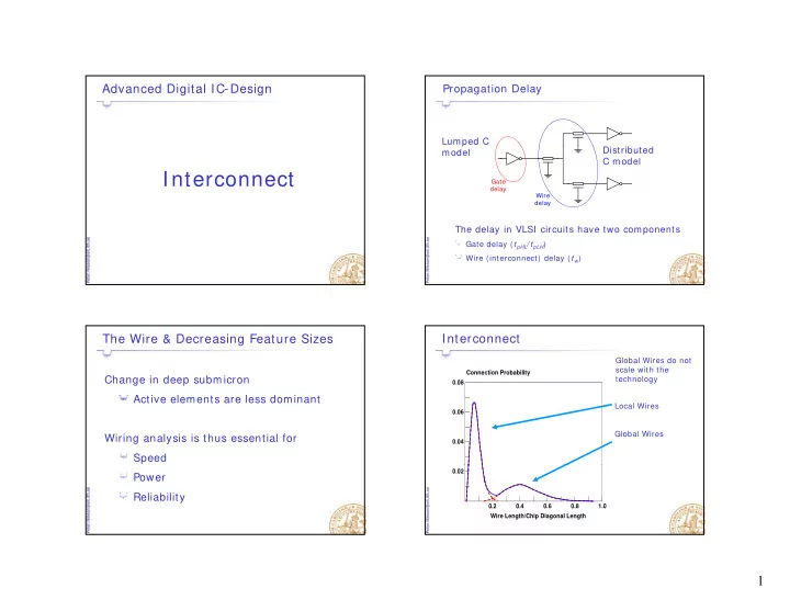
SLIDE 15 15
Leaf Leaf Leaf Leaf Leaf Leaf Leaf
Place & Route (3-10 Metal Layers)
No Routing channels needed
VDD Placement of library cells Routing
Leaf Leaf Leaf Leaf Leaf Leaf Leaf Leaf Cell Leaf Cell Leaf Cell Leaf Cell Leaf Cell Leaf Cell Leaf Cell Cell Cell Cell Cell Cell Cell Cell
GND VDD
Upside-down Leaf Cell Leaf Cell Leaf Cell Leaf Cell Leaf Cell Leaf Cell Leaf Cell Cell Cell Cell Cell Cell Cell Cell
GND VDD
Upside-down
Filler Cell
Leaf Cell Leaf Cell Leaf Cell Leaf Cell Leaf Cell Leaf Cell Leaf Cell Leaf Cell Leaf Cell Leaf Cell Leaf Cell Leaf Cell Leaf Cell Leaf Cell Leaf Cell Leaf Cell Leaf Cell Leaf Cell Leaf Cell Leaf Cell Leaf Cell Leaf Cell Leaf Cell Leaf Cell Leaf Cell Leaf Cell Leaf Cell Leaf Cell
Standard Cells and Macro Cells
Leaf Cell Leaf Cell Leaf Cell Leaf Cell Leaf Cell Leaf Cell Leaf Cell Leaf Cell Leaf Cell Leaf Cell Leaf Cell Leaf Cell Leaf Cell Leaf Cell Leaf Cell Leaf Cell Leaf Cell Leaf Cell Leaf Cell Leaf Cell Leaf Cell Leaf Cell Leaf Cell Leaf Cell Leaf Cell Leaf Cell Leaf Cell Leaf Cell Leaf Cell Leaf Cell Leaf Cell Leaf Cell Leaf Cell Leaf Cell Leaf Cell Leaf Cell Leaf Cell Leaf Cell Leaf Cell Leaf Cell Leaf Cell Leaf Cell
Macro Cell
Macro cells are used for regular structures like RAM: s and sometimes lti li
Leaf Cell Leaf Cell Leaf Cell Leaf Cell Leaf Cell Leaf Cell Leaf Cell Leaf Cell Leaf Cell Leaf Cell Leaf Cell Leaf Cell Leaf Cell Leaf Cell
e.g. Memory
multipliers
Block (power) rings are often used on large blocks
Power and Block Rings (5 Metal Layers)
Separate supply for the pads
RAM
Power rings around the core Bl k i d
Synthesized Block RAM
Block rings around the two blocks (MP3 Accelerator – IC project course)
SoC – A Question of Reuse
Reused Architecture Custom block in
Radio
Embedded RAM
L e a f C e ll Leaf Cell L e a f C e ll L e a f C e ll L e a f C e ll Leaf Cell Leaf Cell L e a f C e ll Leaf Cell L e a f C e ll L e a f C e ll L e a f C e ll Leaf Cell Leaf Cell L e a f C e ll Leaf Cell L e a f C e ll L e a f C e ll L e a f C e ll Leaf Cell Leaf Cell L e a f C e ll Leaf Cell L e a f C e ll L e a f C e ll L e a f C e ll Leaf Cell Leaf Cell L e a f C Leaf Cell L e a f C L e a f C L e a f C Leaf Cell Leaf Cell L e a f C e ll Leaf Cell L e a f C e ll L e a f C e ll L e a f C e ll Leaf Cell Leaf Cell L e a f C e ll Leaf Cell L e a f C e ll L e a f C e ll Leaf Cell Leaf Cell L e a f C e ll Leaf Cell L e a f C e ll L e a f C e ll L e a f C e ll Leaf Cell Leaf Cell L e a f C e ll Leaf Cell L e a f C e ll L e a f C e ll L e a f C e ll Leaf Cell Leaf Cell L e a f C e ll Leaf Cell L e a f C e ll L e a f C e ll L e a f C e ll Leaf Cell Leaf Cell L e a f C e ll Leaf Cell L e a f C e ll L e a f C e ll L e a f C e ll Leaf Cell Leaf Cell L e a f C Leaf Cell L e a f C L e a f C L e a f C Leaf Cell Leaf Cell L e a f C e ll Leaf Cell L e a f C e ll L e a f C e ll L e a f C e ll Leaf Cell Leaf Cell L e a f C e ll Leaf Cell L e a f C e ll L e a f C e ll Leaf Cell Leaf Cell
Acelerator Macro Cell block in Standard Cell Analog IP-Block Analog
Radio Baseband RAM PLL DA
L e a f C e ll Leaf Cell L e a f C e ll L e a f C e ll L e a f C e ll Leaf Cell Leaf Cell L e a f C e ll Leaf Cell L e a f C e ll L e a f C e ll L e a f C e ll Leaf Cell Leaf Cell L e a f C e ll Leaf Cell L e a f C e ll L e a f C e ll L e a f C e ll Leaf Cell Leaf Cell L e a f C e ll Leaf Cell L e a f C e ll L e a f C e ll L e a f C e ll Leaf Cell Leaf Cell L e a f C e ll Leaf Cell L e a f C e ll L e a f C e ll L e a f C e ll Leaf Cell Leaf Cell L e a f C e ll Leaf Cell L e a f C e ll L e a f C e ll L e a f C e ll Leaf Cell Leaf Cell L e a f C e ll Leaf Cell L e a f C e ll L e a f C e ll L e a f C e ll Leaf Cell Leaf Cell L e a f C e ll Leaf Cell L e a f C e ll L e a f C e ll Leaf Cell Leaf Cell L e a f C e ll Leaf Cell L e a f C e ll L e a f C e ll L e a f C e ll Leaf Cell Leaf Cell L e a f C e ll Leaf Cell L e a f C e ll L e a f C e ll L e a f C e ll Leaf Cell Leaf Cell L e a f C e ll Leaf Cell L e a f C e ll L e a f C e ll L e a f C e ll Leaf Cell Leaf Cell L e a f C e ll Leaf Cell L e a f C e ll L e a f C e ll L e a f C e ll Leaf Cell Leaf Cell L e a f C e ll Leaf Cell L e a f C e ll L e a f C e ll L e a f C e ll Leaf Cell Leaf Cell L e a f C e ll Leaf Cell L e a f C e ll L e a f C e ll L e a f C e ll Leaf Cell Leaf Cell L e a f C e ll Leaf Cell L e a f C e ll L e a f C e ll L e a f C e ll Leaf Cell Leaf Cell L e a f C e ll Leaf Cell L e a f C e ll L e a f C e ll Leaf Cell Leaf Cell L e a f C e ll Leaf Cell L e a f C e ll L e a f C e ll L e a f C e ll Leaf Cell Leaf Cell e ll e ll e ll e ll L e a f C e ll Leaf Cell L e a f C e ll L e a f C e ll L e a f C e ll Leaf Cell Leaf Cell e ll e ll e ll e ll
ARM
Processor
RAM
Macro Cell IP Block IP-Block Digital IP-Block IP = Intellectual Property i.e. a block that designed and put on to the market
DA