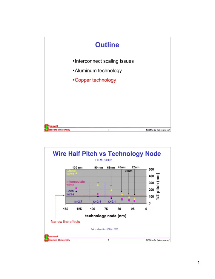
Outline Interconnect scaling issues Aluminum technology Copper - - PDF document

outline
SMART_READER_LITE
LIVE PREVIEW

Outline Interconnect scaling issues Aluminum technology Copper - - PDF document

Outline Interconnect scaling issues Aluminum technology Copper technology araswat tanford University 1 EE311/ Cu Interconnect Wire Half Pitch vs Technology Node ITRS 2002 Narrow line effects Ref: J. Gambino, IEDM, 2003 araswat


slide-1
SLIDE 1

1

EE311/ Cu Interconnect

1 tanford University araswat

Outline

  • Interconnect scaling issues
  • Aluminum technology
  • Copper technology

EE311/ Cu Interconnect

2 tanford University araswat

Wire Half Pitch vs Technology Node

Narrow line effects

Ref: J. Gambino, IEDM, 2003

ITRS 2002

slide-2
SLIDE 2

2

EE311/ Cu Interconnect

3 tanford University araswat 1 1 A1 CS1 1 A1/S 1 SCS1 0.5 0.5 1 1 A1 CS1 1 0.5 CS1 0.5 0.5 A1/S2

Interconnect Scaling Scenarios

  • Scale Metal Pitch with Constant Height
  • R, Cs and J increase by scaling factor
  • Higher aspect ratio for gapfill / metal etch
  • Need for lower resistivity metal, Low-k
  • Scale Metal Pitch and Height
  • R and J increase by square of scaling factor
  • Sidewall capacitance unchanged
  • Aspect ratio for gapfill / metal etch unchanged
  • Need for very low resistivity metal with

significantly improved EM performance

EE311/ Cu Interconnect

4 tanford University araswat

Low ρ (Resistivity)

Metal Ag Cu Au Al W Bulk Resistivity [µΩ•cm] 1.63 1.67 2.35 2.67 5.65

Cu is the second best conducting element

Reduced RC delay

2 3 4 5 6 7 8 9 10 20 30 40 0.1 0.2 0.3 0.4 0.5 0.6

Dealy Time (psec) Feature Size (µm)

50 Cu+Low-k(2.0) Interconnect Delay Gate Delay Al+SiO2 Interconnect Delay Cu+Low-k(2.0) Total Delay Al+SiO2 Total Delay

Calculations assume longest interconnect in the chip controls delay

RC Koxo L2 WH W Xox + H LS

  • Koxo L2

2 for W = H = LS = Xox =

Why Cu and Low-k Dielectrics?

slide-3
SLIDE 3

3

EE311/ Cu Interconnect

5 tanford University araswat

Why Cu and Low-k Dielectrics?

Better electromigration resistance, reduced resistivity and dielectric constant results in reduction in number of metal layers as more wires can by placed in lower levels of metal layers.

global semiglobal local

Ref: M. Bohr, IEDM 1995. 2 4 6 8 10 12 14

Number of Metal Layers Technology Generation (µm)

0.09 0.13 0.18 0.25 0.35 Cu/Low-k Al/Low-k Cu/SiO2 Al/SiO2 EE311/ Cu Interconnect

6 tanford University araswat

Ref: S. Luce, (IBM), IEEE IITC 1998

high electromigration resistance

Al Cu Melting Point 660 ºC 1083 ºC Ea for Lattice Diffusion 1.4 eV 2.2 eV Ea for Grain Boundary Diffusion 0.4 – 0.8 eV 0.7 – 1.2 eV

Why Cu?: Excellent Reliability

Stress Time (hours) Percentile

J = 2.5x10⁶ A/cm2 T = 295°C Cu T50= 147.7 Hrs Al(Cu) T50= 1.31 Hrs

> 110X

slide-4
SLIDE 4

4

EE311/ Cu Interconnect

7 tanford University araswat

Cu atoms ionize, penetrate into the dielectric, and then accumulate in the dielectric as Cu+ space charge.

Problem: Copper Diffusion in Dielectric Films

EE311/ Cu Interconnect

8 tanford University araswat

Copper Diffusion in Dielectric Films

Bias temperature stressing is employed to characterize behavior

  • Both field and temperature affect barrier lifetime
  • Neutral Cu atoms and Cu ions contribute to Cu transport through dielectrics

Ref: A. Loke et al., Symp. VLSI Tech. 1998

Silicon nitride and oxynitride films are better barriers

slide-5
SLIDE 5

5

EE311/ Cu Interconnect

9 tanford University araswat

  • Fast diffusion of Cu into Si and SiO2
  • Poor oxidation/corrosion resistance
  • Poor adhesion to SiO2

Diffusion barrier /adhesion promotor Passivation

  • Difficulty of applying conventional

dry-etching technique Damascene Process

Typical Damascene Process

Dielectrics Barrier Layer

Cu

Solutions to Problems in Copper Metallization

EE311/ Cu Interconnect

10 tanford University araswat

Barriers/Linears

Dielectric Barrier/Linear Metal Via Space for wire

slide-6
SLIDE 6

6

EE311/ Cu Interconnect

11 tanford University araswat

Materials for Barriers / Liners

  • Transition metals (Pd, Cr, Ti, Co, Ni, Pt) generally poor barriers, due to high reactivities to Cu

<450˚C. Exception: Ta, Mo, W ... more thermally stable, but fail due to Cu diffusion through grain boundaries (polycrystalline films)

  • Transition metal alloys: e.g., TiW. Can be deposited as amorphous films (stable up to 500˚C)
  • Transition metal - compounds: Extensively used, e.g., TiN, TaN, WN.
  • Amorphous ternary alloys: Very stable due to high crystallization temperatures (i.e.,

Ta36S14,N50, Ti34Si23N43)

  • Currently PVD (sputtering/evaporation is used primarily to deposit the barrier/liner, however,

step coverage is a problem. ALD is being developed for barrier/liner application.

PVD ALD

EE311/ Cu Interconnect

12 tanford University araswat

Interconnect Fabrication Options

Metal Etch Positive Pattern Dielectric Deposition Dielectric Planarization by CMP Negative Pattern Dielectric Etch Metal Deposition Metal CMP Dielectric Deposition

Metal Dielectric Photoresist Etch Stop (Dielectric)

Subtractive Etch (Conventional Approach) Damascene

slide-7
SLIDE 7

7

EE311/ Cu Interconnect

13 tanford University araswat

Cu Damascene Flow Options

Oxide Copper Conductive Barrier Dielectric Etch Stop/Barrier

Single Damascene Dual Damascene

Barrier & Cu Dep Cu Via CMP Nitride + Oxide Dep Lead Pattern & Etch + Barrier & Cu Dep Via Pattern & Etch Cu Lead CMP Lead Via Via & Lead Pattern & Etch Barrier & Cu Dep Cu CMP Lead Via

EE311/ Cu Interconnect

14 tanford University araswat

Various deposition methods for Cu metallization has been attempted :

 Physical vapor deposition (PVD) : Evaporation, Sputtering

  • conventional metal deposition technique: widely used for Al interconnects
  • produce Cu films with strong (111) texture and smooth surface, in general
  • poor step coverage: not tolerable for filling high-aspect ratio features

Deposition methods of Cu films: PVD

Deposited film

slide-8
SLIDE 8

8

EE311/ Cu Interconnect

15 tanford University araswat

Deposition methods: CVD

 conformal deposition with excellent step coverage in high-aspect ratio holes and vias

  • costly in processing and maintenance
  • generally produce Cu films with fine grain size, weak (111) texture and rough surface

EE311/ Cu Interconnect

16 tanford University araswat

Deposition methods: Electroplating

Dissociation : CuSO4 → Cu2+ + SO42- (solution) Oxidation: Cu → Cu2++ 2e- (anode) Reduction : Cu2+ + 2e- → Cu (cathode, i.e., wafer)

Copper electroplating Chemistry :

  • Plating Bath : standard sulfuric acid

copper sulfate bath (H2SO4, CuSO4 solution)

  • Additives to improve the film quality
slide-9
SLIDE 9

9

EE311/ Cu Interconnect

17 tanford University araswat

 Electrochemical deposition (EVD)

 Good step coverage and filling capability comparable to CVD process (0.25 µm)  Compatible with low-K dielectrics  Generally produce strong (111) texture of Cu film  Produce much larger sized grain structure than any other

deposition methods through self-annealing process

Why Cu Electroplating?

EE311/ Cu Interconnect

18 tanford University araswat

non-conformal "bottom-up filling" ("superfilling")

void

Trench Filling PVD vs. Electroplating of Cu

PVD Electroplating

slide-10
SLIDE 10

10

EE311/ Cu Interconnect

19 tanford University araswat

Seed only 5 seconds 10 seconds 15 seconds 25 seconds

Plated Copper Fill Evolution

Ref: Jonathan Reid, IITC, 1999

EE311/ Cu Interconnect

20 tanford University araswat

Trench Filling Capability of Cu Electroplating

0.13µ trenches 0.18µ vias 029µ vias

Ref: Jonathan Reid, IITC, 1999

slide-11
SLIDE 11

11

EE311/ Cu Interconnect

21 tanford University araswat

Additives for Copper ECD

DEFINITION

  • Mixture of organic molecules and chloride ion which are adsorbed at the

copper surface during plating to:

  • - enhance thickness distribution and feature fill
  • - control copper grain structure and thus ductility, hardness, stress,

and surface smoothness COMPONENTS

  • Most commercial mixtures use 3 or more organic components and

chloride ion which adsorb at the cathode during plating. Brighteners (Accelerators) Levelers Carriers Chloride Suppressors

EE311/ Cu Interconnect

22 tanford University araswat Wafers immersed in plating

  • bath. Additives not yet

adsorbed on Cu seed. Additives adsorbed on Cu

  • seed. No current flow.

Conformal plating begins. Accelerators accumulate at bottom of via, displacing less strongly absorbed additives. Accumulation of accelerator due to reduced surface area in narrow features, causes rapid growth at bottom of via. t = 2 sec t = 10 sec t = 20 sec t = 0 sec = Accelerators = Suppressors c = Chloride ions L = Levelers

Mechanisms of Superconformal Cu plating

Ref: J. Reid et al., Solid St. Tech., 43, 86 (2000)

  • D. Josell et al., J. Electrochem. Soc., 148, C767 (2001)
slide-12
SLIDE 12

12

EE311/ Cu Interconnect

23 tanford University araswat

Brighteners (Accelerators)

  • Adsorbs on copper metal during plating, participates in charge transfer reaction.

Determines Cu growth characteristics with major impact on metallurgy Levelers

  • Reduce growth rate of copper at protrusions and edges to yield a smooth final

deposit surface.

  • Effectively increases polarization resistance at high growth areas by inhibiting

growth to a degree proportional to mass transfer to localized sites Carriers

  • Carriers adsorbed during copper plating to form a relatively thick monolayer film

at the cathode (wafer). Moderately polarizes Cu deposition by forming a barrier to diffusion of Cu2+ ions to the surface. Chloride

  • Adsorbs at both cathode and anode.
  • Accumulates in anode film and increases anode dissolution kinetics.
  • Modifies adsorption properties of carrier to influence thickness distribution.

Role of Additives

EE311/ Cu Interconnect

24 tanford University araswat

Effect of of the seed layer on the properties of the final Cu

Seed Layer Texture Seed Layer Surface Roughness Plated Film Texture Plated Film Texture Plated Film Grain Size

  • Strong (111) texture
  • Smooth surface
  • Strong (111) texture
  • Large grain size

Seed Layer Electroplated Film (Thin, PVD seed preferred)

  • Electroplating needs a seed layer of Cu as it does not occur at a dielectric surface.
  • Properties of the final Cu layer critically depend upon the characteristics of the seed layer.
  • The deposition of the seed layer can be done by PVD, CVD or ALD.
  • Currently PVD is preferred, CVD and ALD being investigated
slide-13
SLIDE 13

13

EE311/ Cu Interconnect

25 tanford University araswat

Electroplated Cu has higher resistance to electromigration because of its grain structure

Electromigration: CVD vs. Electroplating

CVD Cu Electroplated Cu

104 105 106 107 1.8 1.9 2.0 2.1 2.2 2.3

Time-to-Failure (sec) 1/T (10-3/K)

213 °C 238 263 Electroplated Cu Ea = 0.89 eV CVD Cu Ea = 0.82 eV

grain size

e

µ

e

µ

=1.4 µm =0.3 µm

Ref: Ryu, et al., IEEE IRPS 1997. EE311/ Cu Interconnect

26 tanford University araswat

  • Empirical relationship (for Al & Al alloys)

Film Microstructure vs. EM Time-to-Failure

MTF eµ

  • 2 log[ I(111)

I(200) ]

3

10

3

10

4

10

5

10

6

10

7

1.8 1.9 2.0 2.1 2.2 2.3

Time-to-Failure (sec) 1/T (10-3/K)

(111) CVD Cu E

a = 0.86 eV

(200) CVD Cu E

a = 0.81 eV

213 238 263 188°C

  • EM dependence on the microstructure of Cu films
  • S. Vaidya et al.,

Thin Solid Films, Vol. 75, 253, 1981 Ref: Ryu, Loke, Nogami and Wong, IEEE IRPS 1997.

slide-14
SLIDE 14

14

EE311/ Cu Interconnect

27 tanford University araswat

  • W. Steinhögl et al., Phys. Rev. B66 (2002)

Cu Resistivity: Effect of Surface and Grain Boundary Scattering

EE311/ Cu Interconnect

28 tanford University araswat

e e Surface scattering Bulk scattering  Effect of Electron Scattering

  • Reduced mobility as dimensions decrease
  • Grain boundary scattering
  • Surface scattering
  • Reduced mobility as chip temperature increases
  • Increased phonon scattering

Thin Film Resistivity: Role of Carrier Scattering

Grain Grain boundary

slide-15
SLIDE 15

15

EE311/ Cu Interconnect

29 tanford University araswat

  • W. Steinhögl et al., Phys. Rev. B66 (2002)

 Resistivity increases as grain size decreases due to increase in density

  • f grain boundaries which act as carrier scattering sites

 Resistivity increases as main conductor size decreases due to increased surface scattering

Cu Resistivity: Effect of Line Width Scaling Due to Scattering

EE311/ Cu Interconnect

30 tanford University araswat

Cu Resistivity: Effect of Cu diffusion Barrier

Effect of Cu diffusion Barrier

  • Barriers have higher resistivity
  • Barriers can’t be scaled below a minimum thickness
  • Consumes larger area as dimensions decrease

Resistivity of the composite wire is increased Resistivity of metal wires could be much higher than bulk value

Future

Cu Barrier

slide-16
SLIDE 16

16

EE311/ Cu Interconnect

31 tanford University araswat

Cu Resistivity: Integrated Model

Barrier Effect Electron Surface Scattering Effect

w h

  • Important parameter: Ab to Aint ratio
  • ρb increase with Abto Aint ratio
  • Future: ratio may increase

AR=h/w Aint=AR*w2

Cu P: Fraction of electrons scattered elastically from the interface k= d/ λmfp λmfp: Bulk mean free path for electrons d: Smallest dimension of the interconnect Elastic scattering No Change in Mobility Diffuse scattering Lower Mobility P=0 P=1

  • Reduced electron mobility
  • Operational temperature
  • Copper/barrier interface quality
  • Dimensions decrease in tiers: local, semiglobal, global

Barrier Kapur, McVittie & Saraswat, IEEE Trans. Electron Dev. April 2002

s

  • =

1 1 3( 1 P)mfp 2d 1 X

3 1

X

5

  • 1 e

kX

1 Pe

kX dX 1

  • b
  • b

A AR w =

  • 1

1

2

*

EE311/ Cu Interconnect

32 tanford University araswat

Cu Resistivity: Global Interconnects

IPVD C PVD ALD

Effect of Barrier Technology

Cu barrier

  • Barriers can’t be scaled and have very high resistivity
  • Surface electron scattering increases resistivity of scaled wires
  • Real chips operate at higher temperatures

Technology node (µm)

Al

P=0 P=0.5 P=1 Cu, P=0.5

0.18 0.15 0.12 0.1 0.07 0.05 0.035

P V D C

  • P

V D I-PVD ALD: 10nm ALD: 3nm ALD: 1nm No Barrier

Effective resistivity (µ ohm-cm) Year

Kapur and Saraswat, IEEE TED, April 2002

Effect of Scaling

Cu barrier

100°C

e

Al

slide-17
SLIDE 17

17

EE311/ Cu Interconnect

33 tanford University araswat

Semi-global & Local Interconnects

Kapur, McVittie & Saraswat, IEEE Trans. Electron Dev. April 2002

Temp.=100 0C Technology node (µm)

Al P=0 P=0.5 P=1 Cu, P=0.5

0.18 0.15 0.12 0.1 0.07 0.05 0.035

PVD C-PVD A L D : 1 n m A L D : 3 n m A L D : 1 n m No Barrier

Local

Year

Effective resistivity (µ ohm-cm) Local Temp.=100 0C

  • With ALD least resistivity rise
  • Al resistivity rises slower than Cu. Cross over with Cu resistivity possible

– no 4 sided barrier, needs only thin TiN to improve reliability and as anti reflection coating – smaller λmfp => smaller k – But has reliability problem Al

Cu

Technology node (µm)

Al

P=0 P=0.5 P=1

Cu, P=0.5

0.18 0.15 0.12 0.1 0.07 0.05 0.035

PVD C-PVD I

  • P

V D ALD: 10nm ALD: 3nm ALD: 1nm N

  • B

a r r i e r

Semiglobal Temp.=100 0C

EE311/ Cu Interconnect

34 tanford University araswat

  • Higher temperature ⇒ lower mobility ⇒ higher resistivity
  • Realistic Values at 35 nm node: P=0.5, temp=100 0C
  • local ~ 5 µΩ-cm
  • semi-global ~ 4.2 µΩ-cm
  • global ~ 3.2 µΩ-cm

Cu Resistivity: Effect of Chip Temperature

2000 2004 2008 2012 Year 0.18 0.12 0.07 0.05 Technology Node (µm) 0.035 3.6 3.2 2.4 1.6 Effective resistivity (microohm-cm) 2 2.8

T=100 0C T=27 0C

Global

Kapur, McVittie & Saraswat IEEE Trans. Electron Dev. April 2002

slide-18
SLIDE 18

18

EE311/ Cu Interconnect

35 tanford University araswat

Summary

  • Interconnect scaling issues
  • Thermal issues
  • Electromigration
  • Aluminum technology
  • Copper technology