
SLIDE 1
Scaling the Cascades
Interconnect-aware FPGA implementation of Machine Learning problems
Anand Samajdar, Tushar Garg, Tushar Krishna, Nachiket Kapre nachiket@uwaterloo.ca
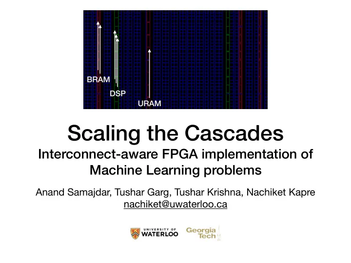
DSP URAM BRAM
Scaling the Cascades Interconnect-aware FPGA implementation of - - PowerPoint PPT Presentation
BRAM DSP URAM Scaling the Cascades Interconnect-aware FPGA implementation of Machine Learning problems Anand Samajdar, Tushar Garg, Tushar Krishna, Nachiket Kapre nachiket@uwaterloo.ca Claim Hard FPGA interconnect (cascades) e ffi ciently
Scaling the Cascades
Interconnect-aware FPGA implementation of Machine Learning problems
Anand Samajdar, Tushar Garg, Tushar Krishna, Nachiket Kapre nachiket@uwaterloo.ca
DSP URAM BRAM
nearest neighbour communication + reuse in ML workloads
, BRAM, URAM]
formidable Xilinx SuperTile design for GoogLeNet v1
4
Landscape of FPGA+ML accelerators
5
Communication Requirements
Input Row k Input Row k+1 Input Row k+2 x x x x x x x x x + Output Row k Input Map I Output Map J Weights
6
Communication Requirements
Input Row k Input Row k+1 Input Row k+2 x x x x x x x x x + Output Row k Input Map I Output Map J pixel streaming row streaming channel streaming 1 2 3 Weights
7
pixel streaming Input Row k+2 x+ x+ x+ Input Row k+1 x+ x+ x+ Input Row k x+ x+ x+
P cascade for summation
Weight Row 2 Weight Row 1 Weight Row 0
8
Input Row k+2 x+ x+ x+ Input Row k+1 x+ x+ x+ Input Row k x+ x+ x+
P cascade for summation A cascade for pixel streaming
Weight Row 2 Weight Row 1 Weight Row 0
B cascade for weight streaming
pixel streaming 1
9
Input Row k+2 x+ x+ x+ Input Row k+1 x+ x+ x+ Input Row k x+ x+ x+
P cascade for summation A cascade for pixel streaming
Weight Row 2 Weight Row 1 Weight Row 0
B cascade for weight streaming Exploit Data Reuse
row streaming 2 pixel streaming 1
10
Input Row k+2 x+ x+ x+ Input Row k+1 x+ x+ x+ Input Row k x+ x+ x+
P cascade for summation A cascade for pixel streaming
Weight Row 2 Weight Row 1 Weight Row 0
B cascade for weight streaming Exploit Data Reuse
row streaming 2 pixel streaming 1 Input Map I Output Map J
11
Input Map I Output Map J 3x3 Convolution Tile
Input Row k Input Row k+1 Input Row k+2 x x x x x x x x x + Output Row k Input Map I Output Map JWeights
12
Input Map I Output Map J 3x3 Convolution Tile Input Map I+1 3x3 Convolution Tile Input Map I+.. 3x3 Convolution Tile Weights Weights Weights
13
Input Map I Output Map J 3x3 Convolution Tile Input Map I+1 3x3 Convolution Tile Input Map I+.. 3x3 Convolution Tile Weights Weights Weights channel streaming 3
14
Input Map I Output Map J 3x3 Convolution Tile Input Map I+1 Input Map I+.. Weights Weights Weights channel streaming 3
15
Xilinx UltraScale+ FPGA Cascades
DSP URAM BRAM
cascades 2x72b-wide links
cascades (systolic input and summation)
cascades
pixel streaming 1 row streaming 2 channel streaming 316
17
General-purpose wiring
architecture
18
cascades
INT8 paper)
(like DSP48E2 user guide)
contribution)
19
need 3 BRAM-long chains
keep one read port available.
20
length-2
cascades
resource ratios, idle cycles available for realizing shifts
21
DSP48 DSP48 DSP48
x +
DSP48
x +
DSP48
x +
DSP48
x +
DSP48
x +
DSP48
x + x + x +
DSP48
x +
22
DSP48 DSP48 DSP48
x +
DSP48
x +
DSP48
x +
DSP48
x +
DSP48
x +
DSP48
x + x + x +
DSP48
x +
23
DSP48 DSP48 DSP48
x +
DSP48
x +
DSP48
x +
DSP48
x +
DSP48
x +
DSP48
x + x + x +
DSP48
x +
Weights (initial shift)
24
DSP48 DSP48 DSP48
x +
DSP48
x +
DSP48
x +
DSP48
x +
DSP48
x +
DSP48
x + x + x +
DSP48
x +
Weights (initial shift) Pixel streaming
25
DSP48 DSP48 DSP48
x +
DSP48
x +
DSP48
x +
DSP48
x +
DSP48
x +
DSP48
x + x + x +
DSP48
x +
RAMB 18 (C) RAMB 18 (B) RAMB 18 (A)
Row i+2 Row i+1 Row i26
Row streaming
DSP48 DSP48 DSP48
x +
DSP48
x +
DSP48
x +
DSP48
x +
DSP48
x +
DSP48
x + x + x +
DSP48
x +
RAMB 18 (C) RAMB 18 (B) RAMB 18 (A)
27
DSP48 DSP48 DSP48
x +
DSP48
x +
DSP48
x +
DSP48
x +
DSP48
x +
DSP48
x + x + x +
DSP48
x +
RAMB 18 (C) RAMB 18 (B) RAMB 18 (A) RAMB 18 (Kern) URAM 288 (Input)
from previous URAM to next URAM(Weights)
28
DSP48 DSP48 DSP48
x +
DSP48
x +
DSP48
x +
DSP48
x +
DSP48
x +
DSP48
x + x + x +
DSP48
x +
RAMB 18 (C) RAMB 18 (B) RAMB 18 (A) RAMB 18 (Kern) URAM 288 (Input)
from previous URAM to next URAM(Weights)
Map streaming
29
DSP48 DSP48 DSP48
x +
DSP48
x +
DSP48
x +
DSP48
x +
DSP48
x +
DSP48
x + x + x +
DSP48
x +
RAMB 18 (C) RAMB 18 (B) RAMB 18 (A) RAMB 18 (Kern) URAM 288 (Input)
from previous URAM to next URAMURAM 288 (Output)
+
(Weights)
30
DSP48 DSP48 DSP48
x +
DSP48
x +
DSP48
x +
DSP48
x +
DSP48
x +
DSP48
x + x + x +
DSP48
x +
RAMB 18 (C) RAMB 18 (B) RAMB 18 (A) RAMB 18 (Kern) URAM 288 (Input)
from previous URAM to next URAMURAM 288 (Output)
+
(Weights)
pixel streaming 1 row streaming 2 channel streaming 3
31
32
33
Places and routes at 1.2ns
34
mix
BRAMs and 9.4 DSP48s
this ratio
DSPs
account for irregular column arrangement of hard resources
35
mix
BRAMs and 9.4 DSP48s
this ratio
DSPs
account for irregular column arrangement of hard resources
ONE TILE
36
Matrix-Matrix Multiplication
result vector to be independently processed.
ring-like fashion —> using BRAM cascades
37
38
CONVOLUTION MATRIX-MULTIPLY
39
CONVOLUTION MATRIX-MULTIPLY
20%
40
20%
41
save us fabric registers for other pipelining needs
utilization
25K 50K 75K 20 40 60 80 Congestion (%) Route Count
Cascade No Cascade
42
save us fabric registers for other pipelining needs
utilization
25K 50K 75K 20 40 60 80 Congestion (%) Route Count
Cascade No Cascade
43
accurate simulator
software/SCALE-Sim
OFMAP SRAMs
=> systolic array links
size 960x9 (conv), 480x9 (mm)
44
VU9P FPGA (Amazon F1)
latency
efficiency
http://isfpga.org/slides/Compute-Efficient_Neural-Network_Acceleration.pdf 45
Why is SuperTile so good?
cascades,
into sub-arrays
layers
significantly boost throughput!
https://dl.acm.org/citation.cfm?id=3293925
46
MLPerf Benchmarks
logo are trademarks. See www.mlperf.org for more information.
47
MLPerf Benchmarks
logo are trademarks. See www.mlperf.org for more information.
48
MLPerf Benchmarks
35 MB URAM Capacity!
logo are trademarks. See www.mlperf.org for more information.
49
50
51
7x Lower Latency
52
53
30% Lower Throughput
LAYER PIPELINING
30% Lower Throughput
54
LAYER PIPELINING
THREE COPIES 30% Lower Throughput
55
56
57
58
59
Xilinx UltraScale+
SuperTile
12% on clock period vs. Fabric interconnect
60
performance suffers due to missing bandwidth from URAM —> Give us 144b ports vs 72b ports!
if data flow in cascades even more programmble —> Give us more control!
Improve DSPs, BRAMs, URAMs + hard interconnect instead—> Stay true to your roots, Xilinx!
61
performance suffers due to missing bandwidth from URAM —> Give us 144b ports vs 72b ports!
if data flow in cascades even more programmble —> Give us more control!
Improve DSPs, BRAMs, URAMs + hard interconnect instead—> Stay true to your roots, Xilinx!
62
Communication Requirements
Vector i+(k-2) Vector i+(k-1) Vector i+k x x x + Partial result vector Matrix Vector i x
63
Communication Requirements
Vector i+(k-2) Vector i+(k-1) Vector i+k x x x + Partial result vector Matrix Vector i x
64
Communication Requirements
Vector i+(k-2) Vector i+(k-1) Vector i+k x x x + Partial result vector Matrix Vector i x Vector fanout 2 Accum stream 1 3 Matrix initialize
65
pixel streaming x+ x+ x+ x+ x+ x+ Vector I x+ x+ x+
P cascade for summation
Matrix
Vector i+(k-2) Vector i+(k-1) Vector i+k x x x + Partial result vector Matrix Vector i xVector i+(k-2) Vector i+(k-1) Vector i+k
66
pixel streaming x+ x+ x+ x+ x+ x+ Vector i x+ x+ x+
P cascade for summation
Matrix
Vector i+(k-2) Vector i+(k-1) Vector i+k x x x + Partial result vector Matrix Vector i xVector i+(k-2) Vector i+(k-1) Vector i+k Accum stream 1
67
pixel streaming x+ x+ x+ x+ x+ x+ Vector i x+ x+ x+
P cascade for summation
Matrix
Vector i+(k-2) Vector i+(k-1) Vector i+k x x x + Partial result vector Matrix Vector i xVector i+(k-2) Vector i+(k-1) Vector i+k Partial Result Accum stream 1
68
pixel streaming x+ x+ x+ x+ x+ x+ Vector i x+ x+ x+
P cascade for summation
Matrix
Vector i+(k-2) Vector i+(k-1) Vector i+k x x x + Partial result vector Matrix Vector i xVector i+(k-2) Vector i+(k-1) Vector i+k Partial Result Accum stream 1 Vector fanout 2
69
pixel streaming x+ x+ x+ x+ x+ x+ Vector i x+ x+ x+
P cascade for summation
Matrix
Vector i+(k-2) Vector i+(k-1) Vector i+k x x x + Partial result vector Matrix Vector i xVector i+(k-2) Vector i+(k-1) Vector i+k Partial Result Accum stream 1 Vector fanout 2 3 Matrix initialize
70
Matrix-Matrix Multiplication
DSP48
x +
DSP48
x +
DSP48
x +
DSP48
x +
DSP48
x +
DSP48
x +
DSP48
x +
DSP48
x +
DSP48
x +
71
Matrix-Matrix Multiplication
DSP48
x +
DSP48
x +
DSP48
x +
DSP48
x +
DSP48
x +
DSP48
x +
DSP48
x +
DSP48
x +
RAMB 18 RAMB 18 RAMB 18 RAMB 18 RAMB 18 RAMB 18 RAMB 18 RAMB 18 DSP48
x +
RAMB 18
72
Matrix-Matrix Multiplication
DSP48
x +
DSP48
x +
DSP48
x +
DSP48
x +
DSP48
x +
DSP48
x +
DSP48
x +
DSP48
x +
RAMB 18 RAMB 18 RAMB 18 RAMB 18 RAMB 18 RAMB 18 RAMB 18 RAMB 18 DSP48
x +
RAMB 18
Vector fanout
73
Matrix-Matrix Multiplication
DSP48
x +
DSP48
x +
DSP48
x +
DSP48
x +
DSP48
x +
DSP48
x +
DSP48
x +
DSP48
x +
RAMB 18 RAMB 18 RAMB 18 RAMB 18 RAMB 18 RAMB 18 RAMB 18 RAMB 18 URAM 288 DSP48
x +
RAMB 18
74
Matrix-Matrix Multiplication
DSP48
x +
DSP48
x +
DSP48
x +
DSP48
x +
DSP48
x +
DSP48
x +
DSP48
x +
DSP48
x +
RAMB 18 RAMB 18 RAMB 18 RAMB 18 RAMB 18 RAMB 18 RAMB 18 RAMB 18 URAM 288 DSP48
x +
RAMB 18
Matrix reads
75
Matrix-Matrix Multiplication
DSP48
x +
DSP48
x +
DSP48
x +
DSP48
x +
DSP48
x +
DSP48
x +
DSP48
x +
DSP48
x +
RAMB 18 RAMB 18 RAMB 18 RAMB 18 RAMB 18 RAMB 18 RAMB 18 RAMB 18 URAM 288
from previous URAM to next URAMDSP48
x +
RAMB 18
76
Matrix-Matrix Multiplication
DSP48
x +
DSP48
x +
DSP48
x +
DSP48
x +
DSP48
x +
DSP48
x +
DSP48
x +
DSP48
x +
RAMB 18 RAMB 18 RAMB 18 RAMB 18 RAMB 18 RAMB 18 RAMB 18 RAMB 18 URAM 288 RAMB 18
+
from previous URAM to next URAMDSP48
x +
RAMB 18
Initial loading
77
MLPerf Benchmarks
logo are trademarks. See www.mlperf.org for more information.
hardware
78
Why is SuperTile so good?
cascades,
sub-arrays
boost throughput!
79
multiplications with a common operand
https://www.xilinx.com/support/documentation/white_papers/wp486-deep-learning-int8.pdf https://www.xilinx.com/support/documentation/white_papers/wp487-int8-acceleration.pdf
80
accumulate multiple product terms
for this length of the chain
accumulations, or if 3x3 convolution support required
https://www.xilinx.com/support/documentation/white_papers/wp486-deep-learning-int8.pdf https://www.xilinx.com/support/documentation/white_papers/wp487-int8-acceleration.pdf
81
Xilinx DSP48 Systolic Mode
https://www.xilinx.com/support/documentation/user_guides/ug479_7Series_DSP48E1.pdf
82