
SLIDE 1
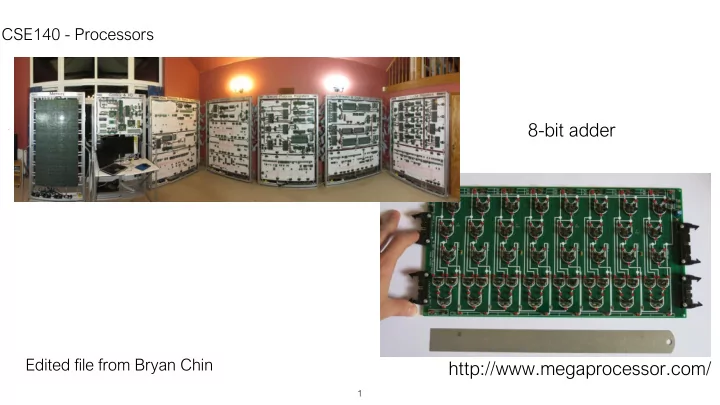
CSE140 - Processors Edited file from Bryan Chin
1
http://www.megaprocessor.com/ 1 Navigation Check Simple (RISC) - - PowerPoint PPT Presentation
CSE140 - Processors 8-bit adder Edited file from Bryan Chin http://www.megaprocessor.com/ 1 Navigation Check Simple (RISC) Processor 2 Simplified Digital Computer Instruction Store Register File Execute Control ALU Memory
1
2
3
ALU Multiply/Divide
4
ALU Add, logic, shift Multiply/Divide
PC
5
Sense Amp Write Driver
WL B+ B-
Memory Cells Memory Cells Memory Cells Memory Cells
Decoder
6
Sense Amp Write Driver
WL B+ B-
Memory Cells Memory Cells Memory Cells Memory Cells
32 rows
Decoder
WAddr[4:0] WE*
Sense Amp
Decoder Decoder
7 Addr[0] Addr[1] Addr[2] Addr[3] Addr[4]
8
9
INSTR STRUCT UCTION ION MEMOR MORY
READ ADDRESS INSTRUCTIO TION [31-0] 0]
MUX
1
MUX
1
ALU LU
ZERO RESULT
DATA TA MEMOR MORY
ADDRESS WRITE TE DATA READ DATA
MUX
1
ADDE DER
RESULT
ADDE DER
RESULT
PC PC MUX
1
4
Sign Extend nd
ALU ALU CONTROL OL
INSTRUCTIO TION[15 15-0] 0] INSTRUCTIO TION[5-0] 0]
<< 2
CON TROL
INSTRUCTI CTION ON[31 31-26] 26] INSTRUCTIO TION[25 25-21] 21] INSTRUCTIO TION[20 20-16] 16] INST[15 15-11] 11] BRANCH REG_DST REG_WRITE RITE ALU_SR SRC ALU_OP OP MEM_READ, D,ME MEM_ M_WRI WRITE TE MEM_TO_R O_REG
REGIST GISTERS ERS
READ REGISTER R 1 READ REGISTER R 2 WRITE TE REGISTER WRITE TE DATA READ DATA 1 READ DATA 2
MUX
1
JUMP
<< 2
I[25-0] 0] JMP ADDRESS [25-0] 0] PC+4 4 [31-28] 8] JMP ADDRESS [31-0] 0]
Src: TSR, Cummings, KFR
10
11
R -Type Opcode Rs Rt Rd Shift (shamt) funct 6 bits 5 bits 5 bits 5 bits 5 bits 6 bits I-Type Opcode Rs Rt Immediate 6 bits 5 bits 5 bits 12 bits J Type Opcode Rs Rt Rd Sa Funct 6 bits 5 bits 5 bits 5 bits 5 bits 6 bits
12
Src: TSR, Cummings, KFR
13
OPCO CODE = 0 RT RT RD RD FUNCT CT = 32 32 or
34 RS RS
Src: TSR, Cummings, KFR
14
INSTR STRUCT UCTION ION MEMOR MORY
READ ADDRESS INSTRUCTIO TION [31-0] 0]
MUX
1
REGIST GISTERS ERS
READ REGISTER R 1 READ REGISTER R 2 WRITE TE REGISTER WRITE TE DATA READ DATA 1 READ DATA 2
MUX
1
ALU LU
ZERO RESULT
DATA TA MEMOR MORY
ADDRESS WRITE TE DATA READ DATA
MUX
1
ADDE DER
RESULT
ADDE DER
RESULT
PC PC MUX
1
4
Sign Extend nd
ALU ALU CONTROL OL
INSTRUCTIO TION[15 15-0] 0] INSTRUCTIO TION[5-0] 0]
<< 2
CON TROL
INSTRUCTIO TION[31 31-26] 26] INSTRUCTIO TION[25 25-21] 21] INSTRUCTIO TION[20 20-16] 16] INST[15 15-11] 11] BRANCH REG_DST REG_WRITE RITE ALU_SR SRC ALU_OP OP MEM_READ, D,ME MEM_ M_WRI WRITE TE MEM_TO_R O_REG
St Step ep 1 (R (R-type): type): Fet etch h inst nstruction ruction an and d ad advan vance ce PC
15
INSTR STRUCT UCTION ION MEMOR MORY
READ ADDRESS INSTRUCTIO TION [31-0] 0]
MUX
1
REGIST GISTERS ERS
READ REGISTER R 1 READ REGISTER R 2 WRITE TE REGISTER WRITE TE DATA READ DATA 1 READ DATA 2
ALU LU
RESULT
DATA TA MEMOR MORY
ADDRESS WRITE TE DATA READ DATA
MUX
1
ADDE DER
RESULT
ADDE DER
RESULT
PC PC MUX
1
4
Sign Extend nd
ALU ALU CONTROL OL
INSTRUCTIO TION[15 15-0] 0] INSTRUCTI CTION ON[5-0] 0]
<< 2
CON TROL
INSTRUCTIO TION[31 31-26] 26] INSTRUCTIO TION[25 25-21] 21] INSTRUCTIO TION[20 20-16] 16] INST[15 15-11] 11] BRANCH REG_DST REG_WRITE RITE ALU_SR SRC ALU_OP OP MEM_READ, D,ME MEM_ M_WRI WRITE TE MEM_TO_R O_REG
St Step ep 2 (R (R-type): type): Rea ead d tw two r
egisters ters an and set et con
trol
gnals ls
ZERO
MUX
1
16
INSTR STRUCT UCTION ION MEMOR MORY
READ ADDRESS INSTRUCTIO TION [31-0] 0]
MUX
1
REGIST GISTERS ERS
READ REGISTER R 1 READ REGISTER R 2 WRITE TE REGISTER WRITE TE DATA READ DATA 1 READ DATA 2
MUX
1
ALU LU
RESULT
DATA TA MEMOR MORY
ADDRESS WRITE TE DATA READ DATA
MUX
1
ADDE DER
RESULT
ADDE DER
RESULT
PC PC MUX
1
4
Sign Extend nd
ALU ALU CONTROL OL
INSTRUCTIO TION[15 15-0] 0] INSTRUCTIO TION[5-0] 0]
<< 2
CON TROL
INSTRUCTIO TION[31 31-26] 26] INSTRUCTIO TION[25 25-21] 21] INSTRUCTIO TION[20 20-16] 16] INST[15 15-11] 11] BRANCH REG_DST REG_WRITE RITE ALU_SR SRC ALU_OP OP MEM_READ, D,ME MEM_ M_WRI WRITE TE MEM_TO_R O_REG
St Step ep 3 (R (R-type): type): Per erform form th the e ALU LU op
eration ation
ZERO
17
INSTR STRUCT UCTION ION MEMOR MORY
READ ADDRESS INSTRUCTIO TION [31-0] 0]
MUX
1
REGIST GISTERS ERS
READ REGISTER R 1 READ REGISTER R 2 WRITE TE REGISTER WRITE TE DATA READ DATA 1 READ DATA 2
MUX
1
ALU LU
RESULT
DATA TA MEMOR MORY
ADDRESS WRITE TE DATA READ DATA
MUX
1
ADDE DER
RESULT
ADDE DER
RESULT
PC PC MUX
1
4
Sign Extend nd
ALU ALU CONTROL OL
INSTRUCTIO TION[15 15-0] 0] INSTRUCTI CTION ON[5-0] 0]
<< 2
CON TROL
INSTRUCTIO TION[31 31-26] 26] INSTRUCTIO TION[25 25-21] 21] INSTRUCTIO TION[20 20-16] 16] INST[15 15-11] 11] BRANCH REG_DST REG_WRITE RITE ALU_SR SRC ALU_OP OP MEM_READ, D,ME MEM_ M_WRI WRITE TE MEM_TO_R O_REG
St Step ep 4 (R (R-type): type): Write te res esult ult to to re register ister
ZERO
18
OPCO CODE = 35 35 or
43 RT RT RS RS
OFFSET ET
19
INSTR STRUCT UCTION ION MEMOR MORY
READ ADDRESS INSTRUCTIO TION [31-0] 0]
MUX
1
REGIST GISTERS ERS
READ REGISTER R 1 READ REGISTER R 2 WRITE TE REGISTER WRITE TE DATA READ DATA 1 READ DATA 2
MUX
1
ALU LU
ZERO RESULT
DATA TA MEMOR MORY
ADDRESS WRITE TE DATA READ DATA
MUX
1
ADDE DER
RESULT
ADDE DER
RESULT
PC PC MUX
1
4
Sign Extend nd
ALU ALU CONTROL OL
INSTRUCTIO TION[15 15-0] 0] INSTRUCTIO TION[5-0] 0]
<< 2
CON TROL
INSTRUCTIO TION[31 31-26] 26] INSTRUCTIO TION[25 25-21] 21] INSTRUCTIO TION[20 20-16] 16] INST[15 15-11] 11] BRANCH REG_DST REG_WRITE RITE ALU_SR SRC ALU_OP OP MEM_READ, D,ME MEM_ M_WRI WRITE TE MEM_TO_R O_REG
St Step ep 1 (s (store tore): ): Fet etch h inst nstruction ruction an and d ad advan vance ce PC
MUX
1
20
INSTR STRUCT UCTION ION MEMOR MORY
READ ADDRESS INSTRUCTIO TION [31-0] 0]
ADDE DER
RESULT
ADDE DER
RESULT
PC PC MUX
1
4
Sign Extend nd
ALU ALU CONTROL OL
INSTRUCTIO TION[15 15-0] 0] INSTRUCTIO TION[5-0] 0]
<< 2
CON TROL
INSTRUCTIO TION[20 20-16] 16] INST[15 15-11] 11] BRANCH REG_DST REG_WRITE RITE ALU_SR SRC ALU_OP OP MEM_READ,ME MEM_ M_WRI WRITE TE MEM_TO_R O_REG
REGIST GISTERS ERS
READ REGISTER R 1 READ REGISTER R 2 WRITE TE REGISTER WRITE TE DATA READ DATA 1 READ DATA 2 INSTRUCTIO TION[15 15-0] 0] INSTRUCTIO TION[31 31-26] 26] INSTRUCTIO TION[25 25-21] 21] INSTRUCTIO TION[20 20-16] 16]
DATA TA MEMOR MORY
ADDRESS WRITE TE DATA READ DATA
ALU LU
RESULT ZERO
MUX
1
St Step ep 2 (s (store tore): ): Rea ead d reg egister ister va values lues an and d set et co control trol signals ignals
MUX
1
MUX
1
21
INSTR STRUCT UCTION ION MEMOR MORY
READ ADDRESS INSTRUCTIO TION [31-0] 0]
ADDE DER
RESULT
ADDE DER
RESULT
PC PC MUX
1
4
Sign Extend nd
ALU ALU CONTROL OL
INSTRUCTIO TION[15 15-0] 0] INSTRUCTIO TION[5-0] 0]
<< 2
CON TROL
INSTRUCTIO TION[20 20-16] 16] INST[15 15-11] 11] BRANCH REG_DST REG_WRITE RITE ALU_SR SRC ALU_OP OP MEM_READ, D,ME MEM_ M_WRI WRITE TE MEM_TO_R O_REG
REGIST GISTERS ERS
READ REGISTER R 1 READ REGISTER R 2 WRITE TE REGISTER WRITE TE DATA READ DATA 1 READ DATA 2 INSTRUCTIO TION[15 15-0] 0] INSTRUCTIO TION[31 31-26] 26] INSTRUCTIO TION[25 25-21] 21] INSTRUCTIO TION[20 20-16] 16]
DATA TA MEMOR MORY
ADDRESS WRITE TE DATA READ DATA
ALU LU
RESULT ZERO
MUX
1
St Step ep 3 (s (store tore): ): Co Compute ute th the e ad address ress
MUX
1
MUX
1
22
INSTR STRUCT UCTION ION MEMOR MORY
READ ADDRESS INSTRUCTIO TION [31-0] 0]
ADDE DER
RESULT
ADDE DER
RESULT
PC PC MUX
1
4
Sign Extend nd
ALU ALU CONTROL OL
INSTRUCTIO TION[15 15-0] 0] INSTRUCTIO TION[5-0] 0]
<< 2
CON TROL
INSTRUCTIO TION[20 20-16] 16] INST[15 15-11] 11] BRANCH REG_DST REG_WRITE RITE ALU_SR SRC ALU_OP OP MEM_READ, D,ME MEM_ M_WRI WRITE TE MEM_TO_R O_REG
REGIST GISTERS ERS
READ REGISTER R 1 READ REGISTER R 2 WRITE TE REGISTER WRITE TE DATA READ DATA 1 READ DATA 2 INSTRUCTIO TION[15 15-0] 0] INSTRUCTIO TION[31 31-26] 26] INSTRUCTIO TION[25 25-21] 21] INSTRUCTIO TION[20 20-16] 16]
DATA TA MEMOR MORY
ADDRESS WRITE TE DATA READ DATA
ALU LU
RESULT ZERO
MUX
1
St Step ep 4 (s (store tore): ): Write te th the e va value lue to to mem memor
MUX
1
MUX
1
23
OPCO CODE = 4 o 4 or r 5 RT RT RS RS
BRANCH TARGET’S OFFSET
24
INSTR STRUCT UCTION ION MEMOR MORY
READ ADDRESS INSTRUCTIO TION [31-0] 0]
MUX
1
REGIST GISTERS ERS
READ REGISTER R 1 READ REGISTER R 2 WRITE TE REGISTER WRITE TE DATA READ DATA 1 READ DATA 2
MUX
1
ALU LU
ZERO RESULT
DATA TA MEMOR MORY
ADDRESS WRITE TE DATA READ DATA
MUX
1
ADDE DER
RESULT
ADDE DER
RESULT
PC PC MUX
1
4
Sign Extend nd
ALU ALU CONTROL OL
INSTRUCTIO TION[15 15-0] 0] INSTRUCTIO TION[5-0] 0]
<< 2
CON TROL
INSTRUCTIO TION[31 31-26] 26] INSTRUCTIO TION[25 25-21] 21] INSTRUCTIO TION[20 20-16] 16] INST[15 15-11] 11] BRANCH REG_DST REG_WRITE RITE ALU_SR SRC ALU_OP OP MEM_READ, D,ME MEM_ M_WRI WRITE TE MEM_TO_R O_REG
St Step ep 1 (b (beq): eq): Fet etch h inst nstruction ruction an and d ad advance vance PC
MUX
1
25
INSTR STRUCT UCTION ION MEMOR MORY
READ ADDRESS INSTRUCTIO TION [31-0] 0]
MUX
1
ADDE DER
RESULT
ADDE DER
RESULT
PC PC
4
Sign Extend nd
ALU ALU CONTROL OL
INSTRUCTIO TION[15 15-0] 0] INSTRUCTIO TION[5-0] 0]
<< 2
CON TROL
INSTRUCTIO TION[20 20-16] 16] INST[15 15-11] 11] BRANCH REG_DST REG_WRITE RITE ALU_SR SRC ALU_OP OP MEM_READ, D,ME MEM_ M_WRI WRITE TE MEM_TO_R O_REG
REGIST GISTERS ERS
READ REGISTER R 1 READ REGISTER R 2 WRITE TE REGISTER WRITE TE DATA READ DATA 1 READ DATA 2 INSTRUCTIO TION[15 15-0] 0] INSTRUCTIO TION[31 31-26] 26] INSTRUCTIO TION[25 25-21] 21] INSTRUCTIO TION[20 20-16] 16]
DATA TA MEMOR MORY
ADDRESS WRITE TE DATA READ DATA
ALU LU
RESULT ZERO
MUX
1
St Step ep 2 (b (beq): eq): Rea ead d regis egister ter va values lues an and d set et con
trol
ignals
MUX
1
MUX
1
26
INSTR STRUCT UCTION ION MEMOR MORY
READ ADDRESS INSTRUCTIO TION [31-0] 0]
MUX
1
ADDE DER
RESULT
ADDE DER
RESULT
PC PC
4
Sign Extend nd
ALU ALU CONTROL OL
INSTRUCTIO TION[15 15-0] 0] INSTRUCTIO TION[5-0] 0]
<< 2
CON TROL
INSTRUCTIO TION[20 20-16] 16] INST[15 15-11] 11] BRANCH REG_DST REG_WRITE RITE ALU_SR SRC ALU_OP OP MEM_READ, D,ME MEM_ M_WRI WRITE TE MEM_TO_R O_REG
REGIST GISTERS ERS
READ REGISTER R 1 READ REGISTER R 2 WRITE TE REGISTER WRITE TE DATA READ DATA 1 READ DATA 2 INSTRUCTIO TION[15 15-0] 0] INSTRUCTIO TION[31 31-26] 26] INSTRUCTIO TION[25 25-21] 21] INSTRUCTIO TION[20 20-16] 16]
DATA TA MEMOR MORY
ADDRESS WRITE TE DATA READ DATA
ALU LU
RESULT ZERO
MUX
1
ew PC
MUX
1
MUX
1
27
OPCO CODE = 2 o 2 or r 3
BR BRANCH CH TA TARGET GET ADDRESS SS
28
INSTR STRUCT UCTION ION MEMOR MORY
READ ADDRESS INSTRUCTIO TION [31-0] 0]
MUX
1
MUX
1
ALU LU
ZERO RESULT
DATA TA MEMOR MORY
ADDRESS WRITE TE DATA READ DATA
MUX
1
ADDE DER
RESULT
ADDE DER
RESULT
PC PC MUX
1
4
Sign Extend nd
ALU ALU CONTROL OL
INSTRUCTIO TION[15 15-0] 0] INSTRUCTIO TION[5-0] 0]
<< 2
CON TROL
INSTRUCTI CTION ON[31 31-26] 26] INSTRUCTIO TION[25 25-21] 21] INSTRUCTIO TION[20 20-16] 16] INST[15 15-11] 11] BRANCH REG_DST REG_WRITE RITE ALU_SR SRC ALU_OP OP MEM_READ, D,ME MEM_ M_WRI WRITE TE MEM_TO_R O_REG
REGIST GISTERS ERS
READ REGISTER R 1 READ REGISTER R 2 WRITE TE REGISTER WRITE TE DATA READ DATA 1 READ DATA 2
MUX
1
JUMP
<< 2
I[25-0] 0] JMP ADDRESS [25-0] 0] PC+4 4 [31-28] 8] JMP ADDRESS [31-0] 0]
Sing ngle le-Cy Cycle le Datapath apath with th Supp pport
mp Instruc tructio ion