
SLIDE 1
EE3032 Introduction to VLSI Design
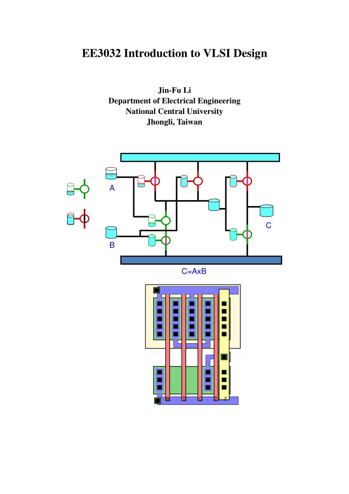
Jin-Fu Li Department of Electrical Engineering National Central University Jhongli, Taiwan
a b c
d
z
A B C C=AxB
EE3032 Introduction to VLSI Design Jin-Fu Li Department of - - PDF document
EE3032 Introduction to VLSI Design Jin-Fu Li Department of Electrical Engineering National Central University Jhongli, Taiwan A C B C=AxB a b c d z Outline Chapter 1: Introduction to CMOS Circuits Chapter 2: MOS Transistor Theory
a b c
d
z
A B C C=AxB
1
Jin-Fu Li Advanced Reliable Systems (ARES) Lab. y m ( E ) L . Department of Electrical Engineering National Central University Jhongli, Taiwan
Advanced Reliable Systems (ARES) Lab. Jin-Fu Li, EE, NCU
2
2
Present state Next state
A a b
a b A B 1 1 1 1 1 1 1 1
B
Advanced Reliable Systems (ARES) Lab. Jin-Fu Li, EE, NCU
3
A = a’b + ab’ B = a’b’ + ab’ CK CLR
Source: Prof. V. D. Agrawal
A B C
Advanced Reliable Systems (ARES) Lab. Jin-Fu Li, EE, NCU
4
B
C=AxB
3
MOSFET: Metal-Oxide-Semiconductor Field- Effect Transistor N-type MOS (NMOS) and P-type MOS (PMOS) Voltage-controlled switches
Advanced Reliable Systems (ARES) Lab. Jin-Fu Li, EE, NCU
5
Using two types of MOSFETs to create logic networks NMOS & PMOS
Silicon is a Group IV element and it forms covalent bonds with four adjacent atoms It i d t
Si Si Si Si Si Si
Si Si +
It is a poor conductor
By introducing small amounts of Group V-As (Group III-B) into the silicon lattice
Advanced Reliable Systems (ARES) Lab. Jin-Fu Li, EE, NCU
6
Si Si Si Si Si Si + As Si Si Si Si Si
Si Si Si Si Si + Lattice of pure Silicon Lattice of N-type Semiconductor Lattice of P-type Semiconductor
4
p-type n-type anode cathode
Advanced Reliable Systems (ARES) Lab. Jin-Fu Li, EE, NCU
7
Gate Source Drain SiO2 Polysilicon
Advanced Reliable Systems (ARES) Lab. Jin-Fu Li, EE, NCU
8
n+ p bulk Si n+
5
P-type body is at low voltage yp y g Source-body and drain-body diodes are OFF No current flows, transistor is OFF
Gate Source Drain SiO2 Polysilicon
Advanced Reliable Systems (ARES) Lab. Jin-Fu Li, EE, NCU
9
n+ p bulk Si n+ D S
Positive charge on gate of MOS capacitor Negative charge attracted to body Inverts a channel under gate to n-type Now current can flow through n-type silicon from source through channel to drain, transistor is ON
Gate Source Drain SiO Polysilicon Advanced Reliable Systems (ARES) Lab. Jin-Fu Li, EE, NCU
10
n+ p bulk Si SiO2 n+ D 1 S
6
Body tied to high voltage (VDD) Gate low: transistor ON Gate high: transistor OFF Bubble indicates inverted behavior
SiO2 Gate Source Drain Polysilicon
Advanced Reliable Systems (ARES) Lab. Jin-Fu Li, EE, NCU
11
n bulk Si p+ p+
T
VDD VA Drain VDD VA
NMOS PMOS
VGSp Source + VDD Advanced Reliable Systems (ARES) Lab. Jin-Fu Li, EE, NCU
12
VA=1 Mn On VA=0 Mn Off VTn Logic translation VA VGSn Mn Source Gate-source voltage Gate +
Mp Off VA=0 Mp On VDD-|VTp| Logic translation VA Drain Mp Gate-source voltage Gate
7
Advanced Reliable Systems (ARES) Lab. Jin-Fu Li, EE, NCU
13
Source: Prof. Banerjee, ECE, UCSB
5v 5v 5v-Vth Vth
0v 0v 5v 0v 0v
th
Vth Vth 5v
Advanced Reliable Systems (ARES) Lab. Jin-Fu Li, EE, NCU
14
8
Transmission gate
C 5 a s b a s b a s b
5 0v
Symbols
Advanced Reliable Systems (ARES) Lab. Jin-Fu Li, EE, NCU
15
5v 0v 5v 0v 5v
Characteristics
F(x)=NOT(x)=x’
Vdd Vin Vout Vin Vout Vdd Vdd Vdd
Advanced Reliable Systems (ARES) Lab. Jin-Fu Li, EE, NCU
16
1 1 Vdd/2 Indeterminate logic level
9
S1
S1=0 S2=0 S1=0 S2=1 S1=1 S2=0 S1=1 S2=1
a S1 1 S1 S2
S1=0 S2=0 S1=0 S2=1 S1=1 S2=0 S1=1 S2=1
b a S2 1 S1 1 a!=b a!=b a!=b a=b
Advanced Reliable Systems (ARES) Lab. Jin-Fu Li, EE, NCU
17
S1 S2 b S2 1 1 a=b a!=b a!=b a!=b
S1=0 S2=0 S1=0 S2=1 S1=1 S2=0 S1=1 S2=1
a S1 S1 S2
S1=0 S2=0 S1=0 S2=1 S1=1 S2=0 S1=1 S2=1
b a S2 1 1 S1 1 a!=b a=b a=b a=b
Advanced Reliable Systems (ARES) Lab. Jin-Fu Li, EE, NCU
18
S1 S2 b S2 1 a=b a=b a=b a!=b
10
A B Output A B 1 1 1 1 1
Advanced Reliable Systems (ARES) Lab. Jin-Fu Li, EE, NCU
19
A B Output
A B Output A B 1 1 1
Advanced Reliable Systems (ARES) Lab. Jin-Fu Li, EE, NCU
20
A B Output
11
( ) (( CD AB F + =
A B A F F C D C A B C D
Advanced Reliable Systems (ARES) Lab. Jin-Fu Li, EE, NCU
21
B D
The output always produces a NOT operation acting on the input variables
VDD f 0 1 1
Advanced Reliable Systems (ARES) Lab. Jin-Fu Li, EE, NCU
22
f=0 a=1
12
Implements the operations in the order AND then OR then NOT E.g.,
d c b a d c b a g . . ) , , , ( + =
Advanced Reliable Systems (ARES) Lab. Jin-Fu Li, EE, NCU
23
Implements the operations in the order OR then AND then NOT E.g.,
) ( ) ( ) , , , ( d c b a d c b a g + ⋅ + =
Parallel-connected nMOS
OR-NOT operations
Parallel-connected pMOS
AND-NOT operations
Series-connected nMOS
AND-NOT operations
Series-connected pMOS
OR-NOT operations
Advanced Reliable Systems (ARES) Lab. Jin-Fu Li, EE, NCU
24
p
13
If an NMOS group yields a function of the form ) ( c b a g + ⋅ = then an identically wired PMOS array gives the dual function where the AND and OR operations have been ) ( c b a G ⋅ + =
Advanced Reliable Systems (ARES) Lab. Jin-Fu Li, EE, NCU
25
p interchanged This is an interesting property of NMOS-PMOS logic that can be exploited in some CMOS designs
( d c b a X + ⋅ + =
VDD a b X b d c Group 1 Group 2 Group 3
Advanced Reliable Systems (ARES) Lab. Jin-Fu Li, EE, NCU
26
a d c
14
Boolean equation of the two input XOR gate
But, , this is in AOI form
b a b a b a ⋅ + ⋅ = ⊕ b a b a b a ⋅ + ⋅ = ⊕
Therefore,
b a b a b a b a ⋅ + ⋅ = ⊕ = ⊕ ) (
VDD a b b a b a ⊕ VDD a b a b b a ⊕
Jin-Fu Li, EE, NCU
27
a b a b a b b a XOR Gate XNOR Gate
A B Y 1 11 10 01 00 A B C D Y A B Y B S
S Y A B C S1 S0
Advanced Reliable Systems (ARES) Lab. Jin-Fu Li, EE, NCU
28
D S1
S0
15
In static circuits at every point in time (except when switching), the output is connected to either Vdd or Gnd through a low resistance path
F i f ( i t ) i 2 ( N t d P
type) devices
Non-ratioed logic: gates operate independent of PMOS or NMOS sizes No path ever exists between Vdd and Gnd: low static power
Advanced Reliable Systems (ARES) Lab. Jin-Fu Li, EE, NCU
29
p Fully-restored logic (NMOS passes “0” only and PMOS passes “1” only Gates must be inverting
Functional, high level For documentation, simulation, verification
System level – CPU, RAM, I/O Functional level – ALU, Multiplier, Adder Gate level – AND, OR, XOR Circuit level – Transistors, R, L, C
Advanced Reliable Systems (ARES) Lab. Jin-Fu Li, EE, NCU
30
For fabrication
16
module fadder(sum,cout,a,b,ci);
input a, b, ci; reg sum, cout; always @(a or b or ci) begin sum = a^b^ci;
ci a b cout sum fadder
Advanced Reliable Systems (ARES) Lab. Jin-Fu Li, EE, NCU
31
cout = (a&b)|(b&ci)|(ci&a); end endmodule
module adder4(s,c4,a,b,ci);
a b
input[3:0] a, b; input ci; reg[3:0] s; reg c4; wire[2:0] co; fadder a0(s[0],co[0],a[0],b[0],ci); fadder a1(s[1] co[1] a[1] b[1] co[0]);
ci a[0] b[0] s[0] a0 a3 a1 a2 a[1] b[1] a[2] b[2] a[3] b[3] s[1] s[2] s3]
co[0] co[1] co[2]
s adder4
Advanced Reliable Systems (ARES) Lab. Jin-Fu Li, EE, NCU
32
fadder a1(s[1],co[1],a[1],b[1],co[0]); fadder a2(s[2],co[2],a[2],b[2],co[1]); fadder a3(s[3],c4,a[3],b[3],co[2]); endmodule
17
Vdd Vdd in1 in2 in3 in4 in1 in2 in3 Out Out
Advanced Reliable Systems (ARES) Lab. Jin-Fu Li, EE, NCU
33
in4 in1 in2 in3 in4 Gnd
Specification Function Behavioral Design Structural Design Function Function Function Timing
Advanced Reliable Systems (ARES) Lab. Jin-Fu Li, EE, NCU
34
Physical Design Timing Power
1
Jin-Fu Li Ad d R li bl S t (ARES) L b Advanced Reliable Systems (ARES) Lab. Department of Electrical Engineering National Central University Jhongli, Taiwan
Advanced Reliable Systems (ARES) Lab. Jin-Fu Li, EE, NCU 2
2
MOS transistors conduct electrical current by using an applied voltage to move charge from the source side to the drain side of the device An MOS transistor is a majority-carrier device m j y In an n-type MOS transistor, the majority carriers are electrons In a p-type MOS transistor, the majority carriers are holes Threshold voltage
Advanced Reliable Systems (ARES) Lab. Jin-Fu Li, EE, NCU 3
to conduct (“turn on”)
MOS transistor symbols
NMOS PMOS
So far, we have treated transistors as ideal switches An ON transistor passes a finite amount of current
i t lt (I V) l ti shi s
Transistor gate, source, drain all have capacitance
The structure of a MOS transistor is symmetric
Advanced Reliable Systems (ARES) Lab. Jin-Fu Li, EE, NCU 4
3
Vg<0
Accumulation mode
Polysilicon Gate Silicon Dioxide Insulator P-type Body 0<Vg<Vt
Depletion mode
Depletion Region
Advanced Reliable Systems (ARES) Lab. Jin-Fu Li, EE, NCU 5
Vg>Vt
Inversion mode
Inversion Region Depletion Region
Vgs=0 Vgd
s d g n+ n+
p-type body
Cutoff region The source and drain have free electrons
Advanced Reliable Systems (ARES) Lab. Jin-Fu Li, EE, NCU 6
he source and dra n have free electrons The body has free holes but no free electrons The junction between the body and the source or drain are reverse-biased, so almost zero current flows
4
Vgs>Vt Vgd=Vgs
s d g s d g n+ n+ n+ n+
Vgs>Vgd>Vt Vgs>Vt
Ids
p-type body p-type body
n+ n+ n+ n+ Vds=0 0<Vds<Vgs-Vt
Linear region A.k.a. resistive, nonsaturated, or unsaturated region If Vgd=Vgs, then Vds=Vgs-Vgd=0 and there is no electrical field
Advanced Reliable Systems (ARES) Lab. Jin-Fu Li, EE, NCU 7
g g g g
tending to push current from drain to source If Vgs>Vgd>Vt, then 0<Vds<Vgs-Vt and there is a small positive potential Vds is applied to the drain , current Ids flows through the channel from drain to source The current increases with both the drain and gate voltage
s d g n+ n+
Vgd<Vt Vgs>Vt
Ids
p-type body
n n Vds>Vgs-Vt Saturation region The Vds becomes sufficiently large that Vgd<Vt, the channel is no longer inverted near the drain and becomes pinched off However conduction is still brought about by the drift of electrons
Advanced Reliable Systems (ARES) Lab. Jin-Fu Li, EE, NCU 8
However, conduction is still brought about by the drift of electrons under the influence of the positive drain voltage As electrons reach the end of the channel, they are injected into the depletion region near the drain and accelerated toward the drain The current Ids is controlled by the gate voltage and ceases to be influenced by the drain
5
If Vgs<Vt, the transistor is cutoff and no current
g
flows If Vgs>Vt and Vds is small, the transistor acts as a linear resistor in which the current flow is proportional to Vds If Vgs>Vt and Vds is large, the transistor acts as a current source in which the current flow becomes
Advanced Reliable Systems (ARES) Lab. Jin-Fu Li, EE, NCU 9
independent of Vds
In linear and saturation regions, the gate attracts carriers to form a channel The carriers drift from source to drain at a rate proportional to the electric field between these proportional to the electric field between these regions MOS structure looks like parallel plate capacitor while
Gate–oxide–channel
Vg
Advanced Reliable Systems (ARES) Lab. Jin-Fu Li, EE, NCU 10
N+ N+
6
Vg C Vs Vd
Qchannel=Cg(Vgc-Vt) , where Cg is the capacitance of the gate to the channel and Vgc-Vt is the amount of voltage
n+ n+ Cg Vc
Advanced Reliable Systems (ARES) Lab. Jin-Fu Li, EE, NCU 11
g
attracting charge to the channel beyond the minimal required to invert from p to n Vc=(Vs+Vd)/2=Vs+Vds/2 Therefore, Vgc=(Vgs+Vgd)/2=Vgs-Vds/2
Transistor dimensions
W tOX Gate
The gate capacitance is
N+ L Gate
WL C ε
Advanced Reliable Systems (ARES) Lab. Jin-Fu Li, EE, NCU 12
g
t C ε =
7
t = L / v
Advanced Reliable Systems (ARES) Lab. Jin-Fu Li, EE, NCU 13
How much charge Qchannel is in the channel How much time t each carrier takes to cross
2 2
ds ds gs t ds ds gs t ds
Q I t W V C V V V L V V V V μ β = ⎛ ⎞ = − − ⎜ ⎟ ⎝ ⎠ ⎛ ⎞ = − − ⎜ ⎟ ⎝ ⎠
Advanced Reliable Systems (ARES) Lab. Jin-Fu Li, EE, NCU 14
Where
2
gs t ds
β ⎜ ⎟ ⎝ ⎠
= W C L β μ
8
When Vds>Vdsat = Vgs–Vt
2
dsat ds gs t dsat gs t
Advanced Reliable Systems (ARES) Lab. Jin-Fu Li, EE, NCU 15
cutoff linear 2
gs t ds ds gs t ds ds dsat
V V V I V V V V V β ⎧ ⎪ < ⎪ ⎪ ⎛ ⎞ = − − < ⎜ ⎟ ⎨ ⎝ ⎠ ⎪
( )
2
saturatio 2 n
gs t ds dsat
V V V V β ⎪ ⎪ − > ⎪ ⎩
1.5 2 2.5
mA) Vgs = 5 Vgs = 4 Vds=Vgs-Vt
Linear Saturation
Advanced Reliable Systems (ARES) Lab. Jin-Fu Li, EE, NCU 16
1 2 3 4 5 0.5 1
Vds Ids (m Vgs = 3 Vgs = 2 Vgs = 1
9
Assume that the parameters of a technology are as follows
2 2.5
Vgs = 5
μ 350 cm /V s
Plot Ids vs. Vds
1 2 3 4 5 0.5 1 1.5
Vds Ids (mA) Vgs = 4 Vgs = 3 Vgs = 2 Vgs = 1 Advanced Reliable Systems (ARES) Lab. Jin-Fu Li, EE, NCU 17
( )
14 2 8
3.9 8.85 10 350 120 / 100 10
W W W C A V L L L β μ μ
− −
⎛ ⎞
⎛ ⎞ = = = ⎜ ⎟ ⎜ ⎟ ⋅ ⎝ ⎠ ⎝ ⎠
Nonideal I-V effects
Velocity saturation, mobility degradation, channel length modulation, subthreshold conduction, body effect, etc.
The saturation current increases less than quadratically i h i i V Thi i d b ff with increasing Vgs. This is caused by two effects:
Velocity saturation Mobility degradation
Velocity saturation
At high lateral field strengths (Vds/L), carrier velocity ceases to increase linearly with field strength R lt i l I th t d t hi h V
Advanced Reliable Systems (ARES) Lab. Jin-Fu Li, EE, NCU 18
Result in lower Ids than expected at high Vds
Mobility degradation
At high vertical field strengths (Vgs/tox), the carriers scatter more often Also lead to less current than expected at high Vgs
10 Ideally, Ids is independent of Vds for a transistor in saturation, making the transistor a perfect current source
2
) ( 2 1
t gs
ds
V V C L W I − = μ
Actually, the width Ld of the depletion region between the channel and drain is increased with Vdb. To avoid introducing the body voltage into our calculations, assume the source voltage is close to the body voltage so Vdb~Vds
Thus the effective channel length is shorten to Leff=L-Ld
2 L
Advanced Reliable Systems (ARES) Lab. Jin-Fu Li, EE, NCU 19
Therefore, the Ids can be expressed as Assume that , then
L L V V C L W V V C L W I
d t gs
t gs
eff ds
− − = − = 1 1 ) ( 2 1 ) ( 2 1
2 2
μ μ
2 2
1 1 ( ) (1 ) ( ) (1 ) 2 2
d ds
gs t
gs t ds
L W W I C V V C V V V L L L μ μ λ = − + = − +
1 << L L d
The parameter is an empirical channel length modulation factor As channel length gets shorter, the effect of the channel length modulation becomes relatively more
λ
channel length modulation becomes relatively more important
Hence is inversely dependent on channel length
This channel length modulation model is a gross
useful for conceptual understanding than for accurate device modeling λ
Advanced Reliable Systems (ARES) Lab. Jin-Fu Li, EE, NCU 20
device modeling Channel length modulation is very important to analog designers because it reduces the gain of amplifiers. It is generally unimportant for qualitatively understanding the behavior of digital circuits
11
Body effect
0 9 0.6 0.65 0.7 0.75 0.8 0.85 0.9
VT (V) Advanced Reliable Systems (ARES) Lab. Jin-Fu Li, EE, NCU 21
0.4 0.45 0.5 0.55
VBS (V)
Degree Low High
It describes the ease with which carriers drift in the substrate material It i d fi d b
It is defined by
Electrons have a higher mobility than holes
Thus NMOS has higher current-producing capability than
μ
Advanced Reliable Systems (ARES) Lab. Jin-Fu Li, EE, NCU 22
Thus NMOS has higher current producing capability than the corresponding PMOS
12
When the drain voltage is high enough, the depletion region around the drain may extend to Th i t t fl i ti
When the source-drain electric field is too large, the electron speed will be high enough to break the electron-hole pair. Moreover, the electrons
Advanced Reliable Systems (ARES) Lab. Jin-Fu Li, EE, NCU 23
p , will penetrate the gate oxide, causing a gate current
Subthreshold region
region, where Ids increases exponentially with Vds and Vgs
Observe in the following figure that at Vgs Vt, the current drops off exponentially rather than abruptly becoming zero
1 mA 100 uA 10 uA 1 uA 100 nA Vds=1.8 Subthreshold region Saturation region
Ids
Advanced Reliable Systems (ARES) Lab. Jin-Fu Li, EE, NCU 24
10 nA 1 nA 100 pA 10 pA 0.3 0.6 0.9 1.2 1.5 1.8
Vgs Vt
Subthreshold slope
13
The p-n junctions between diffusion and the substrate or well form diodes The p-type and n-type substrates are tied to GND or Vdd to ensure these diodes remain reverse-biased However, reverse-biased diodes still conduct a small amount of current IL
(about 26mv at room temperature)
In modern transistors with low threshold voltages, subthreshold conduction far exceeds junction leakage
) 1 ( − =
T D
v V S L
e I I
Advanced Reliable Systems (ARES) Lab. Jin-Fu Li, EE, NCU 25
N+ N+
The magnitude of the threshold voltage decreases nearly linearly with temperature Carrier mobility decreases with temperature Junction leakage increases with temperature because Junction leakage increases with temperature because Is is strongly temperature dependent The following figure shows how the current Idsat decreases with temperature
250 240
Advanced Reliable Systems (ARES) Lab. Jin-Fu Li, EE, NCU 26
230 220 210 20 40 60 80 100 120
Idsat (uA) Temperature (C)
14
The layout designer draws transistors with width and length Wdraw and Ldraw. The actual gate dimensions may differ by some factors XW and XL
polysilicon or may overetch the polysilicon to provide shorter channels (negative XL)
Moreover, the source and drain tend to diffuse laterally under the gate by LD, producing a shorter effective channel length that the carriers must traverse between source and drain. Similarly, diffusion of the bulk by WD decreases the effective channel width
Advanced Reliable Systems (ARES) Lab. Jin-Fu Li, EE, NCU 27
decreases the effective channel width Therefore, the actually effective channel length and width can be expressed as
Gate Drain Cgd Cgs+Cgb Cdb gmVgs gds
(Vsb=0)
Source Linear region Saturation region
2
) ( 2 1
t gs
ds
V V C L W I − = μ ] 2 1 ) [(
2 ds ds t gs
ds
V V V V C L W I − − = μ
Advanced Reliable Systems (ARES) Lab. Jin-Fu Li, EE, NCU 28
) ( 2
t gs
ds
L μ 2
g
L ] ) [(
ds t gs
ds ds ds
V V V C L W dV dI g − − = = μ
ds
ds gs ds m
V C L W const V dV dI g μ = = = .) ( | ) (
t gs
m
V V C L W g − = μ =
ds
g
15 NMOS pass transistor
PMOS pass transistor
Cload Vin S Vout
Advanced Reliable Systems (ARES) Lab. Jin-Fu Li, EE, NCU 29
Cload Vin
Vout
V V
DD
V
DD
V
DD
V
DD
V
DD
Vs = V
DD-V tn
Vs = |V
tp|
V
DD
V
DD-V tn V DD-V tn
V
DD-V tn
V
DD
V
DD
V
DD-V tn
V
DD-2V Advanced Reliable Systems (ARES) Lab. Jin-Fu Li, EE, NCU 30
VSS
DD
V
DD 2V tn
16 By combining behavior of the NMOS and PMOS, we can construct a transmission gate
zero without degradation
g
The transmission gate is a fundamental and ubiquitous component in MOS logic
Cload Vin S Vout
Advanced Reliable Systems (ARES) Lab. Jin-Fu Li, EE, NCU 31
p g
Consider the case where the control input changes rapidly, the Vin is Vdd, and the capacitor on the transmission gate output is discharged (Vss)
he transm ss on gate acts as a res stor
C VDD Vout
Idn+Idp Id
mA
Vss Vdd
Id
Advanced Reliable Systems (ARES) Lab. Jin-Fu Li, EE, NCU 32
Cload S 1 2 3 4 5
Vout
Idp Idn
17 Threshold drops
wrong value: NMOS transistors only pull up to VDD-Vtn, while PMOS transistors only pull down to |Vtp|
body effect
where both 0’s and 1’s must be passed well
VDD
current than expected at high voltage
Advanced Reliable Systems (ARES) Lab. Jin-Fu Li, EE, NCU 33
current than expected at high voltage
to achieve high fast transistors, so VDD has been decreasing with process generation to reduce power consumption
be damaged by high VDD
Leakage current
between source and drain of a transistor that should be cut off
Threshold voltages have been decreasing, so subthreshold leakage has been increasing dramatically
used for high performance, while high-Vt devices are used for low leakage elsewhere
Advanced Reliable Systems (ARES) Lab. Jin-Fu Li, EE, NCU 34
It also limits the amount of time that data is retained in dynamic logic, latches, and memory cells
sort of feedback to prevent data loss from leakage
1
Advanced Reliable Systems (ARES) Lab. Jin-Fu Li, EE, NCU 2
2
Advanced Reliable Systems (ARES) Lab. Jin-Fu Li, EE, NCU 3
It is an excellent electrical insulator It can be grown on a silicon wafer or deposited on t f th f
top of the wafer Thermal oxide
Si+O2SiO2 (dry oxidation), using heat as a catalyst
Si+2H2OSiO2+2H2 (wet oxidation)
The surface of the silicon is recessed from its original
Advanced Reliable Systems (ARES) Lab. Jin-Fu Li, EE, NCU 4
The surface of the silicon is recessed from its original location
CVD oxide
SiH4(gas)+2O2(gas)SiO2(solid)+2H2O(gas) Chemical vapor deposition (CVD)
3
A.k.a. nitride 3SiH4(gas)+4NH3(gas)Si3N4(solid)+12H2(gas)
Nitrides act as strong barriers to most atoms, this makes them ideal for use as an overglass layer
Called polysilicon or just poly for short It is used as the gate material in MOSFETs SiH Si 2H
Advanced Reliable Systems (ARES) Lab. Jin-Fu Li, EE, NCU 5
SiH4Si+2H2 It adheres well to silicon dioxide
Aluminum (Al) is the most common metal used for interconnect wiring in ICs
It is pr ne t electr mi rati n
It is prone to electromigration J=I/A; A=wt is the cross-section area Layout engineers cannot alter the thickness t of the layer Electromigration is thus controlled by specifying the minimum width w to keep J below a max. value
Copper (Cu) has recently been introduced as a
Advanced Reliable Systems (ARES) Lab. Jin-Fu Li, EE, NCU 6
pp ( ) y replacement to aluminum
Its resistivity is about one-half the value of Al Standard patterning techniques cannot be used on copper layers; specialized techniques had to be developed
4
Doped Silicon Layers
process
p y p p yp the wafer surface
Basic section of an ion implanter
Ion source Accelerator Magnetic Mass Separator
Advanced Reliable Systems (ARES) Lab. Jin-Fu Li, EE, NCU 7
Ion beam wafer
The process of deposition causes that the top surface has hillocks
will get increasing rough and may lead to breaks in fine line g g g y features and other problems
Chemical-Mechanical Polishing (CMP)
sanding to produce planar surfaces on silicon wafers
Surface planarization
Advanced Reliable Systems (ARES) Lab. Jin-Fu Li, EE, NCU 8
poly substrate substrate
5
l
Photolithography
Advanced Reliable Systems (ARES) Lab. Jin-Fu Li, EE, NCU 9
Coat photoresist
Coat photoresist Exposure step Etching
Liquid photoresist is sprayed onto a spinning wafer
Advanced Reliable Systems (ARES) Lab. Jin-Fu Li, EE, NCU 10
Photoresist is sensitive to light, such as ultraviolet (UV)
6
UV mask Hardened resist layer
regions from the etching process
E hi
wafer a photoresist wafer resist layer
Advanced Reliable Systems (ARES) Lab. Jin-Fu Li, EE, NCU 11
Etching
layer not shielded by the hardened photoresist
Hardened resist layer Patterned
Creation of doped silicon
Substrate Oxide layer Substrate Arsenic ions
Advanced Reliable Systems (ARES) Lab. Jin-Fu Li, EE, NCU 12
Substrate Substrate N+ N+ Lateral dopping
7
Advanced Reliable Systems (ARES) Lab. Jin-Fu Li, EE, NCU 13
Basic structure of a NMOS transistor
Advanced Reliable Systems (ARES) Lab. Jin-Fu Li, EE, NCU 14
8
p-substrate Patterning SiO2 Layer p-substrate n+ n+ Implant or Diffusion
Implant of
p p-substrate p-substrate p-substrate n+ n+ Gate Oxidation Contact Cuts
Thin Oxide Polysilicon Impurities SiO2 by deposition Al contacts
Advanced Reliable Systems (ARES) Lab. Jin-Fu Li, EE, NCU 15
p-substrate p-substrate n+ n+ Patterning Polysilicon Patterning Al layer
N-well process P-well process
Twin-tub process Silicon on insulator (SOI)
Starts with a lightly doped p-type (n-type) substrate (wafer), create the n-type (p-type) well f th h l ( h l) d i d b ild
Advanced Reliable Systems (ARES) Lab. Jin-Fu Li, EE, NCU 16
for the p-channel (n-channel) devices, and build the n-channel (p-channel) transistor in the native p-substrate (n-substrate)
9
n-well mask
Mask (top view) Cross Section of Physical Structure n-well p-substrate n-well
active mask
Advanced Reliable Systems (ARES) Lab. Jin-Fu Li, EE, NCU 17
p-substrate
nitride
Active n-well
channel stop mask Resist Implant (Boron) p-channel stop
p-substrate Channel stop n-well
Advanced Reliable Systems (ARES) Lab. Jin-Fu Li, EE, NCU 18
p-substrate n-well
10
polysilicon mask
p-substrate n-well
n+ mask
polysilicon
Advanced Reliable Systems (ARES) Lab. Jin-Fu Li, EE, NCU 19
p-substrate n-well n+ n+ n+ mask
Light implant heavier implant
poly poly
n- n- n+ n+ n- n-
Shadow drain implant LDD (lightly doped drain) structure poly p+ mask
Advanced Reliable Systems (ARES) Lab. Jin-Fu Li, EE, NCU 20
p-substrate n-well n+ n+ p+ p+ p+ mask
11
contact mask
p-substrate n-well n+ n+ p+ p+
metal mask
contact mask
Advanced Reliable Systems (ARES) Lab. Jin-Fu Li, EE, NCU 21
p-substrate n-well n+ n+ p+ p+ metal mask
in Vdd Vss
in
Advanced Reliable Systems (ARES) Lab. Jin-Fu Li, EE, NCU 22
Vdd Vss
12
n+ n+ p+ p+ p-substrate n-well n+ n+ p p
field oxide gate oxide metal polysilicon contact cut
Advanced Reliable Systems (ARES) Lab. Jin-Fu Li, EE, NCU 23
p-substrate n-well n+ n+ p+ p+
Advanced Reliable Systems (ARES) Lab. Jin-Fu Li, EE, NCU 24
13
Provide a necessary communication link between circuit designers and process engineers during f t i h
manufacturing phase The goal of design rules is to achieve the optimum yield of a circuit with the smallest area cost
Advanced Reliable Systems (ARES) Lab. Jin-Fu Li, EE, NCU 25
The geometrical reproduction of features that can be reproduced by the mask-making and lith hi l
lithographical process The interactions between different layers
Based on a single parameter, lambda, which characterizes the linear feature – the resolution
Advanced Reliable Systems (ARES) Lab. Jin-Fu Li, EE, NCU 26
14
9 W ll Different Potential Same Potential 10 Well Active 3 3 Polysilicon 2 2 3
6
Advanced Reliable Systems (ARES) Lab. Jin-Fu Li, EE, NCU 27
Metal1 3 3 2 Contact
2 Hole
1 2 3 T ransisto
Advanced Reliable Systems (ARES) Lab. Jin-Fu Li, EE, NCU 28
5
15
1 Via 1 2 4 1 2 1 Metal to Poly Contact Metal to Active Contact 1 5 3 2 2
Advanced Reliable Systems (ARES) Lab. Jin-Fu Li, EE, NCU 29
2
Advanced Reliable Systems (ARES) Lab. Jin-Fu Li, EE, NCU 30
16
Advanced Reliable Systems (ARES) Lab. Jin-Fu Li, EE, NCU 31
p+ p+ p+ n+ n+ n+ Rwell NPN PNP Vdd N-well Rsubstrate
well
Rwell 2.0mA I P-substrate
Advanced Reliable Systems (ARES) Lab. Jin-Fu Li, EE, NCU 32
Rsubstrate Holding Voltage Trigger point Iramp Iramp 1 2 3 4
Vne Vne
17
Lateral triggering & vertical triggering
Advanced Reliable Systems (ARES) Lab. Jin-Fu Li, EE, NCU 33
well npn
pnp ntrigger
R V I α
−
≈
Latchup resistant CMOS process Layout techniques
Advanced Reliable Systems (ARES) Lab. Jin-Fu Li, EE, NCU 34
Reducing the gain of parasitic transistors is achieved through the use of guard rings
18
p+ l emitter Vdd
Advanced Reliable Systems (ARES) Lab. Jin-Fu Li, EE, NCU 35
N-well n+ p-plus n-plus n-plus base collector (substrate)
A p+ guard ring is shown below for an n+ source/drain
p+ + p+ n+ Vss
A n+ guard ring is shown below for a p+ source/drain
N-well + + +
hole current P+ collects hole current thereby shielding n+ source/drain n+ collects electron current th b hi ldi +
Vdd
Advanced Reliable Systems (ARES) Lab. Jin-Fu Li, EE, NCU 36
p+ N-well
n+
thereby shielding p+ source/drain
dd
n+
19 When a metal wire contacted to a transistor gate is plasma-etched, it can charge up to a voltage sufficient to break down thin gate oxide The metal can be contacted to diffusion to provide a
The metal can be contacted to diffusion to provide a path for the charge to bleed away Antenna rules specify the maximum area of metal that can be connected to a gate without a source or drain to act as a discharge element The design rule normally defines the maximum ratio f t l t t h th t h th
Advanced Reliable Systems (ARES) Lab. Jin-Fu Li, EE, NCU 37
metal will not damage the gate
thickness of the gate oxide (and hence breakdown voltage)
L2
Length L2 exceeds allowed limit Wire attracts charge during plasma processing and builds up voltage V=Q/C Any source/drain can act as a discharge element discharge element Gate may be connected to source/drain at any metal layer in an auto routing situation
metal 4 Advanced Reliable Systems (ARES) Lab. Jin-Fu Li, EE, NCU 38
Added link solves problem-L1 satisfies design rule
metal 1 metal 2 metal 3
L1
20
An alternative method is to attach source/drain diodes to problem nets as shown below
substrate rather than transistor source/drain regions
Antenna diode may be added
L2
Advanced Reliable Systems (ARES) Lab. Jin-Fu Li, EE, NCU 39
For advanced processes, a minimum and maximum density of a particular layer within a specific area should be specified
Layer density rules are required as a result of the CMP process and the desire to achieve uniform etch rates For example, a metal layer might have to have 30% minimum and 70% maximum fill within a 1mm by 1mm area For digital circuits layer density levels are normally
Advanced Reliable Systems (ARES) Lab. Jin-Fu Li, EE, NCU 40
For digital circuits, layer density levels are normally reached with normal routing Analog & RF circuits are almost sparse
fill program after design has been completed
21
Multiple threshold voltages
t
p g
t
elsewhere to limit leakage power
various thresholds
Silicon on insulator (SOI) process
T j d t li i ti f th it b t
Advanced Reliable Systems (ARES) Lab. Jin-Fu Li, EE, NCU 41
the source/drain regions and body, leading to higher-speed devices; lower subthreshold leakage
High-k gate dielectrics
channel→very thin SiO2 gate dieletrics
Scaling trends indicate the gate leakage will be Scaling trends indicate the gate leakage will be unacceptably large in such thin gates
material with a higher dielectric constant were available
Advanced Reliable Systems (ARES) Lab. Jin-Fu Li, EE, NCU 42
22
Advanced Reliable Systems (ARES) Lab. Jin-Fu Li, EE, NCU 43
Advanced Reliable Systems (ARES) Lab. Jin-Fu Li, EE, NCU 44
Source: Proceedings of IEEE, Jan. 2009
23
(1) Before CMOS (2) After CMOS & BEOL
Advanced Reliable Systems (ARES) Lab. Jin-Fu Li, EE, NCU 45
Source: Yole, 2007.
(2) After CMOS & BEOL
(1) After BEOL & before bonding (2) After bonding
Advanced Reliable Systems (ARES) Lab. Jin-Fu Li, EE, NCU 46
Source: Yole, 2007.
24
Advanced Reliable Systems (ARES) Lab. Jin-Fu Li, EE, NCU 47
Source: ASP-DAC 2009.
Advanced Reliable Systems (ARES) Lab. Jin-Fu Li, EE, NCU 48
Source: ASP-DAC 2009.
25
Advanced Reliable Systems (ARES) Lab. Jin-Fu Li, EE, NCU 49
Source: ASP-DAC 2009.
H h f
Advanced Reliable Systems (ARES) Lab. Jin-Fu Li, EE, NCU 50
Source: Proceedings of IEEE, Jan. 2009
26
Advanced Reliable Systems (ARES) Lab. Jin-Fu Li, EE, NCU 51
Source: Proceedings of IEEE, Jan. 2009
1
Jin-Fu Li Department of Electrical Engineering Department of Electrical Engineering National Central University Jungli, Taiwan
Resistance & Capacitance Estimation DC Response Logic Level and Noise Margins
Transient Response Delay Estimation Transistor Sizing Power Analysis Scaling Theory
Advanced Reliable Systems (ARES) Lab. Jin-Fu Li, EE, NCU 2
2
thickness, conductor length, conductor width)
) / )( / ( W L t R ρ = ) , , , ( W L t ρ
Thus ) / ( W L R R
s
=
W W W L t
/ Ω =
s
R
1 rectangular block ) / ( W L R R
s
=
Advanced Reliable Systems (ARES) Lab. Jin-Fu Li, EE, NCU 3
W L L L t 4 rectangular block ) / ( ) 2 / 2 ( W L R W L R R
s s
= =
RC model of an NMOS
R G
The drain-source resistance at any point on the current curve as shown below
D S CD Cs Rn D S G
Advanced Reliable Systems (ARES) Lab. Jin-Fu Li, EE, NCU 4
Vds I ds a b c
3
The current is approximated by
t gs n ds
V V V I ) ( − ≈ β Thus the resistance is
The full non-saturated current must be used so that
( / 1
t gs n n
V V R − ≈ β
g
] ) ( 2 [ 1
2 d d d
V V V V I − − = β
Advanced Reliable Systems (ARES) Lab. Jin-Fu Li, EE, NCU 5
) ( 2 [ / 2
ds t gs n n
V V V R − − = β
] ) ( 2 [ 2
ds ds t gs n ds
V V V V I β
The current is
2
) ( 2 1
t gs n ds
V V I − ≈ β
Thus the resistance is
2
) ( / 2
t gs n ds n
V V V R − = β
β
Advanced Reliable Systems (ARES) Lab. Jin-Fu Li, EE, NCU 6
n n
R β / 1 ∝
) / ( L W k
n =
β
n
β
4
Gate capacitance Diffusion capacitance R ti it
Advanced Reliable Systems (ARES) Lab. Jin-Fu Li, EE, NCU 7
Routing capacitance
A d C
x
ε ε 0 =
x
ε ε
Advanced Reliable Systems (ARES) Lab. Jin-Fu Li, EE, NCU 8
Accumulation Depletion Inversion
5
The negative charge on the gate attracts holes toward the silicon surface Th MOS t t b h lik ll l l t The MOS structure behaves like a parallel-plate capacitor
gate gate Co tox Vg<0
A C
SiO 2 0ε
ε
Advanced Reliable Systems (ARES) Lab. Jin-Fu Li, EE, NCU 9
P-substrate
t C
SiO 2 0 =
The positive gate voltage repels holes, leaving a ti l h d i d l t d f i negatively charged region depleted of carriers
gate gate Co C
Depletion layer
tox Vg~0
d
A d C
Si dep
ε ε 0 =
Advanced Reliable Systems (ARES) Lab. Jin-Fu Li, EE, NCU 10
P-substrate Cdep
dep dep gb
C C C C C + =
6
If the MOS is operated at high frequency, the f h i t bl t t k f t i surface charge is not able to track fast moving gate voltages
gate gate Co C
Depletion layer
tox Vg>0
Channel
C C gb =
Low frequency Hi h f
Advanced Reliable Systems (ARES) Lab. Jin-Fu Li, EE, NCU 11
P-substrate Cdep
Depletion layer
min
C C C C C C
dep dep gb
= + =
High frequency
Accumulation Depletion Inversion
Vgs V 1.0 C/Co
Accumulation Depletion Inversion
Low freq. High freq.
Advanced Reliable Systems (ARES) Lab. Jin-Fu Li, EE, NCU 12
Vgs Vt
7
Cgs, Cgd: gate-to-channel capacitances, which are l d t th d th d i i f th lumped at the source and the drain regions of the channel, respectively Csb, Cdb: source and drain-diffusion capacitances to bulk Cgb: gate-to-bulk capacitance
gate Cdb Cgd
Advanced Reliable Systems (ARES) Lab. Jin-Fu Li, EE, NCU 13
Csb Cdb Cgd Cgb Cgs
depletion layer
substrate
source drain Cg=Cgb+Cgs+Cgd
channel
Csb Cgb Cgs
Off region (Vgs<Vt): Cgs=Cgd=0; Cg=Cgb Non-saturated region (Vgs-Vt>Vds): Cgs and Cgd become significant. These capacitances are dependent on gate voltage. Their value can be estimated as
A C C
SiO d
2
1 ε ε = =
Advanced Reliable Systems (ARES) Lab. Jin-Fu Li, EE, NCU 14
Saturated region (Vgs-Vt<Vds): The drain region is pinched off, causing Cgd to be zero. Cgs increases to approximately
A t C C
gs gd
2 A t C
SiO
2
3 2 ε ε =
8
SiO
t C
2
ε ε = A C C
g =
m μ
8
10 150
−
×
λ 2
Advanced Reliable Systems (ARES) Lab. Jin-Fu Li, EE, NCU 15
pF pF C g 005 . 10 2 5 . 25 2 10 150 10 854 . 8 9 . 3
4 8 14
≈ × × = × × × × =
− − −
λ 2 m μ λ 5 . = λ 5
λ 4
Substrate
b a
Source Diffusion Area Drain Diffusion Area
b a
Xc (a finite depth)
Cjp
Advanced Reliable Systems (ARES) Lab. Jin-Fu Li, EE, NCU 16
Cja ) 2 2 ( ) ( b a C ab C C
jp ja d
+ × + × = Cja=junction capacitance per micron square Cjp=periphery capacitance per micron
9
V
Advanced Reliable Systems (ARES) Lab. Jin-Fu Li, EE, NCU 17
b
V
m b j j j
V V C C
−
− = ) 1 (
j
C
j
C
V 6 . ~ =
j
V
W L T Fringing fields H substrate Insulator (Oxide)
Advanced Reliable Systems (ARES) Lab. Jin-Fu Li, EE, NCU 18
substrate ( )
10
The capacitance interactions between layers can become quite complex
Layer 3 Layer 2
C23 C22
Multi-layer d t
Advanced Reliable Systems (ARES) Lab. Jin-Fu Li, EE, NCU 19
Layer 2 Layer 1
C21
C2=C21+C23+C22
conductor
B C A D F G E B C A D F G E
m2 m2 m2 m2 m2 m2 m1 m1 m1
C C C C C
poly poly
Advanced Reliable Systems (ARES) Lab. Jin-Fu Li, EE, NCU 20
C C C C C
Thin-oxide/diffusion
Substrate
poly poly
11
) 4 ln( 2 d h L π μ =
h d w
) 4 8 ln( 2 h w w h L + = π μ
h w
Advanced Reliable Systems (ARES) Lab. Jin-Fu Li, EE, NCU 21
dt di L V =
Vj-1 Vj Vj+1 Ij-1 Ij
R C R C R C R C R C
Advanced Reliable Systems (ARES) Lab. Jin-Fu Li, EE, NCU 22
The response at node Vj with respect to time is then given by
V V R V V I I dt dV C Idt CdV
j j j j j j j
) ( ) ( ) (
1 1 1 + − −
− − − = − = ⇒ =
12
2 2 2
kx t dx V d dt dV rc
x =
⇒ =
c r : resistance per unit length
: capacitance per unit length
Advanced Reliable Systems (ARES) Lab. Jin-Fu Li, EE, NCU 23
) 1 ( 7 . + × = n RCn tn 2 7 .
2 1
rcl t =
Assume that With buffer
2 15
10 4 x tx
−
× =
2 15 2 15
1000 10 4 1000 10 4 × × + + × × =
− − buf p
t t
b f b f
t ns ns t ns + = + + = 8 4 4
Advanced Reliable Systems (ARES) Lab. Jin-Fu Li, EE, NCU 24
Without buffer By keeping the buffer delay small, significant gain can be obtained with buffer insertion
buf buf
t ns ns t ns + + + 8 4 4 ns t p 16 2000 10 4
2 15
= × × =
−
13
When the neighbor switches from 1-> 0 or 0->1, the wire tends to switch too. Called capacitive coupling or crosstalk.
Noise on nonswitching wires d d l h
Advanced Reliable Systems (ARES) Lab. Jin-Fu Li, EE, NCU 25
Increased delay on switching wires
Second terminal of capacitor can be ignored Model as Cgnd = Ctop + Cbot
Miller effect A B
B ΔV Ceff(A) MCF
Advanced Reliable Systems (ARES) Lab. Jin-Fu Li, EE, NCU 26
A B
Cadj Cgnd Cgnd Constant VDD Cgnd + Cadj 1 Switching with A Cgnd Switching opposite A 2VDD Cgnd + 2 Cadj 2
14
model as capacitive voltage divider
Aggressor adj victim aggressor gnd v adj
−
Advanced Reliable Systems (ARES) Lab. Jin-Fu Li, EE, NCU 27
Cadj Cgnd-v Victim ΔVaggressor ΔVvictim
Noise depends on relative resistances Victim driver is in linear region, agg. in saturation If sizes are same, Raggressor = 2-4 x Rvictim
1 1
adj victim aggressor gnd v adj
C V V C C k
−
Δ = Δ + +
Cadj Aggressor ΔVaggressor Raggressor Cgnd-a Advanced Reliable Systems (ARES) Lab. Jin-Fu Li, EE, NCU 28
( ) ( )
aggressor gnd a adj aggressor victim victim gnd v adj
R C C k R C C τ τ
− −
+ = = +
adj
Cgnd-v Victim ΔVvictim Rvictim
15
Aggressor
1.8 Victim (undriven): 50% Victim (half size driver): 16% 0.6 0.9 1.2 1.5
Advanced Reliable Systems (ARES) Lab. Jin-Fu Li, EE, NCU 29
Victim (equal size driver): 8% Victim (double size driver): 4%
t (ps)
200 400 600 800 1000 1200 1400 1800 2000 0.3
When Vin = 0 Vout=VDD
in
DD
When Vin = VDD Vout=0 In between, Vout depends on transistor size and current By KCL, must settle such that Idsn = |Idsp| Idsn Idsp Vout VDD Vin
Advanced Reliable Systems (ARES) Lab. Jin-Fu Li, EE, NCU 30
p
We could solve equations But graphical solution gives more insight
16
Advanced Reliable Systems (ARES) Lab. Jin-Fu Li, EE, NCU 31
Cutoff Linear Saturated Vgsn < Vtn Vgsn > Vtn Vgsn > Vtn Vdsn < Vgsn – Vtn Vdsn > Vgsn – Vtn
I VDD
Advanced Reliable Systems (ARES) Lab. Jin-Fu Li, EE, NCU 32
Idsn Idsp Vout Vin
Vgsn = Vin Vdsn = Vout
17
Cutoff Linear Saturated
Vgsn < Vtn Vi < Vt Vgsn > Vtn Vi > Vt Vgsn > Vtn Vi > Vt Vin < Vtn Vin > Vtn Vdsn < Vgsn – Vtn Vout < Vin - Vtn Vin > Vtn Vdsn > Vgsn – Vtn Vout > Vin - Vtn
I VDD
V V
Advanced Reliable Systems (ARES) Lab. Jin-Fu Li, EE, NCU 33
Idsn Idsp Vout Vin
Vgsn = Vin Vdsn = Vout
Cutoff Linear Saturated Vgsp > Vtp Vgsp < Vtp Vgsp < Vtp Vdsp > Vgsp – Vtp Vdsp < Vgsp – Vtp
Idsp V VDD V
V = V
V
V < 0
Advanced Reliable Systems (ARES) Lab. Jin-Fu Li, EE, NCU 34
Idsn
dsp
Vout Vin
Vgsp = Vin - VDD Vdsp = Vout - VDD Vtp < 0
18
Cutoff Linear Saturated Vgsp > Vtp Vin > VDD + Vtp Vgsp < Vtp Vin < VDD + Vtp Vgsp < Vtp Vin < VDD + Vtp Vdsp > Vgsp – Vtp Vout > Vin - Vtp Vdsp < Vgsp – Vtp Vout < Vin - Vtp
I VDD
V = V
V
V < 0
Advanced Reliable Systems (ARES) Lab. Jin-Fu Li, EE, NCU 35
Idsn Idsp Vout Vin
Vgsp = Vin - VDD Vdsp = Vout - VDD Vtp < 0
Vgsn5 Vgsn4 Vgsn3 Vgsn2 Vgsn1 V Vgsp2 Vgsp1 VDD
V
Idsn
Advanced Reliable Systems (ARES) Lab. Jin-Fu Li, EE, NCU 36
Vgsp5 Vgsp4 Vgsp3 Vdsn
19
Vin5 Vin1 Vin4 Vin3 Vin2 Vin2 Vin3 Vin4 Idsn, |Idsp|
Advanced Reliable Systems (ARES) Lab. Jin-Fu Li, EE, NCU 37
in2
Vin1
in4
Vin5 Vout VDD
Plot Idsn, Idsp vs. Vout Vout must be where |currents| are equal in
Idsp V VDD V
Vin5 Vin4 V Vin1 Vin2 V Idsn, |Idsp|
Advanced Reliable Systems (ARES) Lab. Jin-Fu Li, EE, NCU 38
Idsn Vout Vin
Vin3 Vin2 Vin1 Vin3 Vin4 Vin5 Vout VDD
20
Vin5 Vin4 Vin1 Vin2 VDD A B Vin3 Vin2 Vin1 Vin3 Vin4 Vin5 V
VDD
Advanced Reliable Systems (ARES) Lab. Jin-Fu Li, EE, NCU 39
C Vout Vin VDD D E
Vtn VDD/2 VDD+Vtp
C Vout VDD A B D
Region nMOS pMOS A Cutoff Linear B Saturation Linear C Saturation Saturation D Linear Saturation
Advanced Reliable Systems (ARES) Lab. Jin-Fu Li, EE, NCU 40
Vin VDD D E
Vtn VDD/2 VDD+Vtp
E Linear Cutoff
21
Vout VDD 1 2
10
p n
β β =
Advanced Reliable Systems (ARES) Lab. Jin-Fu Li, EE, NCU 41
Vin VDD 0.5
0.1
p n
β β =
Indeterminate Region NMH Input Characteristics Output Characteristics VOH VDD VIH V Logical High Input Range Logical High Output Range
Advanced Reliable Systems (ARES) Lab. Jin-Fu Li, EE, NCU 42
Region NML VOL GND VIL Logical Low Input Range Logical Low Output Range
22
Advanced Reliable Systems (ARES) Lab. Jin-Fu Li, EE, NCU 43
V (t) V (t) Vin(t) Vout(t) Vin(t) VDD CL Ids Vds=Vgs-Vt
Advanced Reliable Systems (ARES) Lab. Jin-Fu Li, EE, NCU 44
Vout(t) tdf tdr 90% 50% 10% tf tr VDD t t Vout(t) VDD
23
The time for a waveform to rise from 10% to 90%
The time for a waveform to fall from 90% to 10% steady-state value
The time difference between input transition (50%) and the 50% output level (This is the time
Advanced Reliable Systems (ARES) Lab. Jin-Fu Li, EE, NCU 45
(50%) and the 50% output level. (This is the time taken for a logic transition to pass from input to
High-to-low delay (tdf) Low-to-high delay (tdr)
PMOS PMOS
t i d d i hi h th it lt V
Idsn
NMOS NMOS
Saturated Vout>=VDD-Vtn Nonsaturated 0<Vout<=VDD-Vtn Vout(t) Vout(t) Rcn CL CL
Input rising
Advanced Reliable Systems (ARES) Lab. Jin-Fu Li, EE, NCU 46
tf1=period during which the capacitor voltage, Vout, drops from 0.9VDD to (VDD-Vtn) tf2=period during which the capacitor voltage, Vout, drops from (VDD-Vtn) to 0.1VDD
24
( 2
2 =
− +
tn DD n
L
V V dt dV C β
tf2 also can be obtained by the same way Finally, the fall time can be estimated with
dt
DD n L f
V C k t β × ≈
DD p L r
V C k t β × ≈
Advanced Reliable Systems (ARES) Lab. Jin-Fu Li, EE, NCU 47
1 1 (
p n DD L p
V C k t β β + × ≈
p
, rise time=fall time
This implies Wp=2-3Wn
Reduce CL
n
β
p
β
L
Careful layout can help to reduce the diffusion and interconnect capacitance
Increase and
Increase the transistor sizes also increases the diffusion capacitance as well as the gate capacitance. The latter will increase the fan out factor of the
n
β
p
β
Advanced Reliable Systems (ARES) Lab. Jin-Fu Li, EE, NCU 48
The latter will increase the fan-out factor of the driving gate and adversely affect its speed
Increase VDD
Designers don’t have too much control over this
25
IN 3 P3 P2 P1 N
When pull-down path is conducting
IN-2 IN-1 N3 N2 N1
) / 1 ( ) / 1 ( ) / 1 ( 1
3 2 1 n n n neff
β β β β + + =
Advanced Reliable Systems (ARES) Lab. Jin-Fu Li, EE, NCU 49
For
When the pull-down path is conducting
Only one p-transistor has to turn on to raise the output. Thus 3
3 2 1 n neff n n n
β β β β β = ⇒ = =
p peff
β β =
In n l th f ll tim t is mt (t /m) f m n
L L L 3L w w
Advanced Reliable Systems (ARES) Lab. Jin-Fu Li, EE, NCU 50
In general, the fall time tf is mtf (tf/m) for m n- transistors in series (parallel). Similarly the rise time tr for k p-transistors in series (parallel) is ktr (tr/k)
26
Transistors are regarded as a resistance discharging or charging a capacitance
Lumped RCs
Distributed RCs
Rp Rn C
−
× =
path pulldown pulldown df
C R t
Advanced Reliable Systems (ARES) Lab. Jin-Fu Li, EE, NCU 51
i i d
C R t
=
Simple RC model
−
× =
path pulldown pulldown df
C R t
Elmore RC model
P4 P3 P2 P1 N4 N3 A B Cab C Cout
p p p f
) ( ) (
4 3 2 1 cd bc ab
N N N N
C C C C R R R R + + + × + + + =
p dr
C R t × =
4 i i i d
C R t
=
Advanced Reliable Systems (ARES) Lab. Jin-Fu Li, EE, NCU 52
N2 N1 C D Cbc Ccd
] ) [( ] ) [( ) (
3 2 1 2 1 1 ab N N N bc N N cd N df
C R R R C R R C R t × + + + × + + × = ] ) [(
4 3 2 1
N N N N
C R R R R × + + + +
27
As discussed above, if we want to have approximately the same rise and fall times for an inverter, for current CMOS process, we must m k make
Wp =2-3Wn Increase layout area and dynamic power dissipation
In some cascaded structures it is possible to use minimum or equal-size devices without
Advanced Reliable Systems (ARES) Lab. Jin-Fu Li, EE, NCU 53
minimum or equal size devices without compromising the switching response In the following, we illustrate two examples to explain why it is possible
Example 1:
I h tinv-pair 4/1
rise fall pair inv
C R C R t t t 3 2 3 + =
−
Example 2:
Icharge Idischarge 3Ceq Wp=2Wn 3Ceq 4/1 2/1
R R
eq eq
C C R 3 2 2 3 + =
eq eq
RC RC 3 3 + =
eq
RC 6 =
tinv-pair
Advanced Reliable Systems (ARES) Lab. Jin-Fu Li, EE, NCU 54
Icharge Idischarge 2Ceq Wp=Wn 2Ceq
inv pair
2/1 2/1
2R R eq eq rise fall pair inv
C R C R t t t 2 2 2 + = + =
− eq
RC 6 =
28
To drive large capacitances such as long buses, I/O buffers, etc.
Using a chain of inverters where each successive inverter is made larger than the previous one until inverter is made larger than the previous one until the last inverter in the chain can drive the large load in the time required The ratio by which each stage is increased in size is called stage ratio
Consider the circuit shown below
Advanced Reliable Systems (ARES) Lab. Jin-Fu Li, EE, NCU 55
It consists of n-cascaded inverters with stage- ratio a driving a capacitance CL
1 a a2 a3 CL n(4) stages
The delay through each stage is atd, where td is the average delay of a minimum-sized inverter driving another minimum-sized inverter H th d l th h st s is t Hence the delay through n stages is natd If the ratio of the load capacitance to the capacitance of a minimum inverter, CL/Cg, is R, then an=R
Hence ln(R)=nln(a) Thus the total delay is ln(R)(a/ln(a))td
Advanced Reliable Systems (ARES) Lab. Jin-Fu Li, EE, NCU 56
Thus the total delay is ln(R)(a/ln(a))td The optimal stage ratio may be determined from
a a k
e a
+
=
gate drain
C C
29
Instantaneous power
The value of power consumed at any given instant
k ) ( ) ( ) ( t i t v t P = Peak power
The highest power value at any given instant; peak power determines the component’s thermal and electrical limits and system packaging requirements
peak peak
Vi P =
Advanced Reliable Systems (ARES) Lab. Jin-Fu Li, EE, NCU 57
Average power
The total distribution of power over a time period; average power impacts the battery lifetime and heat dissipation
+ +
= =
T t t T t t ave
dt t i T V dt t P T P ) ( ) ( 1
Static power dissipation
d b h l k d h Caused by the leakage current and other static current
Dynamic power dissipation
Caused by the total output capacitance Caused by the short-circuit current
Advanced Reliable Systems (ARES) Lab. Jin-Fu Li, EE, NCU 58
power; Psc: short-circuit power
sc sw s t
P P P P + + =
30
Reverse bias leakage between diffusion regions and the substrate Subthreshold conduction
KT qV
e i i
/
) 1 ( =
PN junction reverse bias leakage current
VDD Vin Vout Gnd p+ p+ p+ n+ n+ n+
Advanced Reliable Systems (ARES) Lab. Jin-Fu Li, EE, NCU 59
ply n leakage s s
V I P e i i
sup 1
) 1 ( × = − =
p-substrate n-well n=number of devices
Caused by charging and discharging the output capacitive load
Vin Vout VDD ip
=
T
dt t v t i T P ) ( ) ( 1
dv C i i dt dv C i i
= = = =
Advanced Reliable Systems (ARES) Lab. Jin-Fu Li, EE, NCU 60
Vin CL in io
dt C i i
L
− = − =
] [ 1
− =
DD DD
V V
sw
dv v C dv v C T P
2 2 DD L DD L sw
V fC T V C P = =
31
The energy drawn from the power supply is
DD
V →
2
The Ecap is consumed by the pull-down NMOS
2
2 1
DD L
cap
V C dv v C E
DD
= = ∫
2 DD LV
C QV E = =
→
DD
V
Advanced Reliable Systems (ARES) Lab. Jin-Fu Li, EE, NCU 61
Minimize the product of power and delay
Even if there were no load capacitance on the
negligible, the gate still dissipate switching energy f h h l l b h h N d If the input changes slowly, both the NMOS and PMOS transistors are ON, an excess power is dissipated due to the short-circuit current We are assuming that the rise time of the input is equal to the fall time The short circuit power is estimated as
Advanced Reliable Systems (ARES) Lab. Jin-Fu Li, EE, NCU 62
The short-circuit power is estimated as
mean sc
V I P =
32
VDD
tr tf T VDD-|Vt | Vin
Vin Vout CL
isc
r f
VDD |Vtp| Vtn Imax Imean
Advanced Reliable Systems (ARES) Lab. Jin-Fu Li, EE, NCU 63
t1 t2 t3
] ) ( [ 4 ] ) ( ) ( [ 1 2
2 1 2 1 3 2
= + × =
t t mean t t t t mean
dt t i T I dt t i dt t i T I
dt V t V I
t
β
2
] ) ) ( ( [ 4
2
t t t V V t t t V t V dt V t V T I
r r DD T r DD in T in t mean
β
2 1 2
) ( ] ) ) ( ( 2 [
1
= = = − =
Advanced Reliable Systems (ARES) Lab. Jin-Fu Li, EE, NCU 64
f V V P t
T DD sc
τ β
3 2
) 2 ( 12 2 − =
) ( τ = =
f r
t t
33
Internal cell power Capacitive load power
DD L L 2
B C VDD C1 A
Advanced Reliable Systems (ARES) Lab. Jin-Fu Li, EE, NCU 65
DD i i n i i
=
1 int
C2 B C A
D A B ABC D 100 111
Advanced Reliable Systems (ARES) Lab. Jin-Fu Li, EE, NCU 66
C Z Z Unit delay Spurious transition
34
Advanced Reliable Systems (ARES) Lab. Jin-Fu Li, EE, NCU 67
DD L L 2
Recent years have seen an acceleration in supply voltage reduction
DD i i i i
=
1 int
Advanced Reliable Systems (ARES) Lab. Jin-Fu Li, EE, NCU 68
Design at very low voltage still open question (0.6V…0.9V by 2010)
35
Identify, in your circuit, the high switching nodes Keep the wires of high activity nodes short Use low-capacitance layers (e.g., metal2, metal 3, etc ) for high capacitive nodes and busses etc.) for high capacitive nodes and busses Avoid, if possible, the use of dynamic logic design style For any logic design, reduce the switching activity, by logic reordering and balanced delays through gate tree to avoid glitch problem I iti l th i i i d i
Advanced Reliable Systems (ARES) Lab. Jin-Fu Li, EE, NCU 69
In non-critical paths, use minimum size devices whenever it is possible without degrading the
If pass-transistor logic style is used, careful design should be considered
Electromigration Power supply noise and integrity (i.e., satisfactory d i l lt l l t d t power and signal voltage levels are presented to each gate) RC delay
Current density Temperature
Advanced Reliable Systems (ARES) Lab. Jin-Fu Li, EE, NCU 70
Temperature Crystal structure
m mA J Al μ / 2 1 → =
36
Voltage Vin Current Time Time L VDD Pad VSS Pad Vout Vin Vout I I
Advanced Reliable Systems (ARES) Lab. Jin-Fu Li, EE, NCU 71
VL=L(di/dt) Time L VSS Pad VL Ground bounce
Multiple power and ground pins
Restrict the number of I/O drivers connected to a single supply pins (reduce the di/dt per supply pin)
Careful selection of the position of the power and ground pins on the package
Avoid locating the power and ground pins at the corners of the package (reduce the L)
Increase the rise and fall times
Reduce the di/dt
Advanced Reliable Systems (ARES) Lab. Jin-Fu Li, EE, NCU 72
Reduce the di/dt
Adding decoupling capacitances on the board
Separate the bonding-wire inductance from the inductance of the board interconnect
37
This effect, called current crowding, puts a ti l li it th i f th t t practical upper limit on the size of the contact When a contact or a via between different layers is necessary, make sure to maximize the contact perimeter (not area)
Advanced Reliable Systems (ARES) Lab. Jin-Fu Li, EE, NCU 73
A bus can be modeled as a capacitor Cb An element attached to the bus can be modeled as a capacitor Cs
Bus
Advanced Reliable Systems (ARES) Lab. Jin-Fu Li, EE, NCU 74
Vb Cb Vs Cs
) (
b b b
V C Q = ) (
s s s
V C Q =
s s b b T
V C V C Q + =
s b T
C C C + = ) /( ) (
s b s s b b T T R
C C V C V C C Q V + + = =
38
The operating condition of a chip is influenced by three major factors
Operating temperature S l lt Supply voltage Process variation
One must aim to design a circuit that will reliably
variables Design corners
Advanced Reliable Systems (ARES) Lab. Jin-Fu Li, EE, NCU 75
Design corners
Simulating circuits at all corners is needed
SS TT FF
Packaging requirements
Electrical: low parasitics Mechanical: reliable and robust h l ff h l Thermal: efficient heat removal Economical: cheap
Bonding techniques
Substrate
Wire Bonding
Advanced Reliable Systems (ARES) Lab. Jin-Fu Li, EE, NCU 76 Lead Frame Substrate Die Pad
39
% 100 per wafer chips
number Total per wafer chips good
No. × = Y t W f yield Die per wafer Dies cost Wafer cost Die × =
area die 2 diameter wafer area die diameter/2 wafer per wafer Dies
2
× × π − × π =
Advanced Reliable Systems (ARES) Lab. Jin-Fu Li, EE, NCU 77
Single die
Advanced Reliable Systems (ARES) Lab. Jin-Fu Li, EE, NCU 78
Going up to 12” (30cm)
40
S W W = ~ S L L = ~
Advanced Reliable Systems (ARES) Lab. Jin-Fu Li, EE, NCU 79
~ S A A = L W L W ~ ~ =
The oxide capacitance is given by
d d th th l d d i h
t C ε = t ~
decreased as , then the scaled device has The transconductance is increased in the scaled device to
S t t
~
SC C = ~ β β S = ~
Advanced Reliable Systems (ARES) Lab. Jin-Fu Li, EE, NCU 80
S R V V S R
T DD
= − = ) ( 1 ~ β
41
On the other hand, if we can scale the voltages in the scaled device to the new values of
S V V
DD DD =
~ S V V
T T =
~
The resistance of the scaled device would be unchanged with
The effects of scaling the voltage, consider a scaled MOS with reduced voltages of
S V V
DS DS =
~
R R = ~
S V V
GS GS =
~
Advanced Reliable Systems (ARES) Lab. Jin-Fu Li, EE, NCU 81
f g y
I S V S V S V S I
D DS T GS D
= − = ] ) [( 2 ~ β
2 2
~ ~ ~ S P S I V I V P
D DS D DS
= = =
Advanced Reliable Systems (ARES) Lab. Jin-Fu Li, EE, NCU 82
1
Jin-Fu Li Advanced Reliable Systems (ARES) Lab Advanced Reliable Systems (ARES) Lab. Department of Electrical Engineering National Central University Jhongli, Taiwan
Advanced Reliable Systems (ARES) Lab. Jin-Fu Li, EE, NCU 2
2
The actual process of creating circuits on silicon During this phase, schematic diagrams are carefully translated into sets of geometric patterns that are d t d fi th hi h i l t t
used to define the on-chip physical structures
A graphics program that allows the designer to specify
Advanced Reliable Systems (ARES) Lab. Jin-Fu Li, EE, NCU 3
A graph cs program that allows the des gner to spec fy the shape, dimensions, and placement
The gates constitute cells in the library
This process is called instantiate of the cell A copy of a cell is called an instance
Advanced Reliable Systems (ARES) Lab. Jin-Fu Li, EE, NCU 4
Small changes in the shapes or area of a polygon will affect the resulting electrical characteristics
3
Simplify the procedure and aid in the verification process
Layout editor Extraction routine Layout versus schematic (LVS) l h k ( )
Advanced Reliable Systems (ARES) Lab. Jin-Fu Li, EE, NCU 5
Design rule checker (DRC) Place and route routine Electrical rule checker (ERC)
Start with P-type substrate nWell Active Poly pSelect nSelect Active Contact Poly contact
Advanced Reliable Systems (ARES) Lab. Jin-Fu Li, EE, NCU 6
Poly contact Metal1 Via Metal2 …
4
For example,
w
Advanced Reliable Systems (ARES) Lab. Jin-Fu Li, EE, NCU 7
S
NMOS
L Poly L Poly
PMOS
n+ n+ P n+ n+ W L Poly L Poly
Advanced Reliable Systems (ARES) Lab. Jin-Fu Li, EE, NCU 8
p+ p+ N-well Poly p+ p+ W P N-well
5
Vdd Vout Vin Vin Vout Vdd
Advanced Reliable Systems (ARES) Lab. Jin-Fu Li, EE, NCU 9
Vss Vss
Vdd Vdd a z a z b
Advanced Reliable Systems (ARES) Lab. Jin-Fu Li, EE, NCU 10
Vss a Vss b
6
Vdd Vdd z a z b
Advanced Reliable Systems (ARES) Lab. Jin-Fu Li, EE, NCU 11
a Vss b Vss
Vdd Vdd Vss Vss in
Vdd Vdd Vss Vss in1
in2 Vdd Vdd Vss Vss in1
in2 XNOT XNAND2 XNOR2
Advanced Reliable Systems (ARES) Lab. Jin-Fu Li, EE, NCU 12
Note that power supply ports for Vdd and Vss are chosen to be at the same locations for every cell The width of each cell depends on the transistor sizes and wiring used at the physical level
7
f=a’b
Vdd Vss a f b 2XNOT+ XNAND2
Advanced Reliable Systems (ARES) Lab. Jin-Fu Li, EE, NCU 13
Vdd Vss a b f
NOT NAND2
Vdd
D : edge to edge distance between V and V
Vss nWell PMOSs NMOSs P-substrate Dm1-m1 Pm1-m1
Advanced Reliable Systems (ARES) Lab. Jin-Fu Li, EE, NCU 14
Dm1-m1: edge-to-edge distance between Vdd and Vss Pm1-m1: distance between the middle of the Vdd and Vss lines Pm1-m1=Dm1-m1+Wdd, where Wdd is the width of the power supply lines
8
Vdd WP Wn WP Wn
Advanced Reliable Systems (ARES) Lab. Jin-Fu Li, EE, NCU 15
Vss
Vdd
A B C D Vss
Advanced Reliable Systems (ARES) Lab. Jin-Fu Li, EE, NCU 16
A B C D Vdd Vss
9
Interconnection routing considerations are very important considerations for the Vss-Vdd spacing
In complex digital systems, the wiring is often more complicated than designing the transistor arrays p g g y The general idea for routing
Metal1 Wiring Vdd Vss Vdd
cell1 cell2 cell3 cell4 cell5
Routing Channel
Metal2 Metal3 Wiring
Advanced Reliable Systems (ARES) Lab. Jin-Fu Li, EE, NCU 17
Metal1 Wiring Vss Vdd Vss
cell6 cell10 cell7 cell8 cell9 cell13 cell12 cell11
Routing Channel
Metal2 Wiring
For example,
V
Since no space is automatically reserved for routing
Vdd Vss Vdd Vss Logic cells Inverted logic cells Logic cells Inverted logic cells Vdd
Advanced Reliable Systems (ARES) Lab. Jin-Fu Li, EE, NCU 18
Since no space is automatically reserved for routing, this scheme allows for high-density of placement of cells The main drawback is that the connection between rows must be accomplished by using Metal2 or higher
10
V PMOS transistors Vdd Vss nWell P-substrate P-substrate PMOS transistors NMOS transistors NMOS transistors
Advanced Reliable Systems (ARES) Lab. Jin-Fu Li, EE, NCU 19
Vdd nWell PMOS transistors PMOS transistors
Metal1
Metal1 input Vdd
Advanced Reliable Systems (ARES) Lab. Jin-Fu Li, EE, NCU 20
To routing channel Vss
11
L L L W 2W 4W X 2X 4X
Advanced Reliable Systems (ARES) Lab. Jin-Fu Li, EE, NCU 21
W L L 2W X 2X
C D Vdd A Z B A B C D C z Vdd Vss
Advanced Reliable Systems (ARES) Lab. Jin-Fu Li, EE, NCU 22
D
ss
A B C D
12
A B Z Z’ z Vdd Z’ Z’ A B A B
Advanced Reliable Systems (ARES) Lab. Jin-Fu Li, EE, NCU 23
Vss A B Z’
A B Z z Vdd Vss B
Advanced Reliable Systems (ARES) Lab. Jin-Fu Li, EE, NCU 24
A
13
A B E D C E A B E D C Vdd E Vdd Vss A B E D C A B E D C P
Advanced Reliable Systems (ARES) Lab. Jin-Fu Li, EE, NCU 25
Vss P N
WVdd Wp Dnp
Advanced Reliable Systems (ARES) Lab. Jin-Fu Li, EE, NCU 26
Wn WVss a b c z d
14
Vdd Vdd
Advanced Reliable Systems (ARES) Lab. Jin-Fu Li, EE, NCU 27
Vss Vss a b c a b c z z
Vdd
Advanced Reliable Systems (ARES) Lab. Jin-Fu Li, EE, NCU 28
Vss
15
Vdd Gate array cells
Advanced Reliable Systems (ARES) Lab. Jin-Fu Li, EE, NCU 29
Vss Routing channels
Vdd supply well contacts P-transistors poly gates P-transistors
Advanced Reliable Systems (ARES) Lab. Jin-Fu Li, EE, NCU 30
Vss supply substrate contacts N-transistors
16
a b c z a b c z
Advanced Reliable Systems (ARES) Lab. Jin-Fu Li, EE, NCU 31
a b c
Advanced Reliable Systems (ARES) Lab. Jin-Fu Li, EE, NCU 32
DD
17
Advanced Reliable Systems (ARES) Lab. Jin-Fu Li, EE, NCU 33
Vary the size of the transistor according to the position in the structure
clk Vdd F A<0> A<1> A<2> A<3> F Vss
Advanced Reliable Systems (ARES) Lab. Jin-Fu Li, EE, NCU 34
In submicron technologies, where the source/drain capacitances are less, such that this improvement is limited
A<0> A<1> A<2> A<3> clk
18
D B A D B C 2 Z A C
Z Vdd
Right Wrong
D 1 Advanced Reliable Systems (ARES) Lab. Jin-Fu Li, EE, NCU 35
Z A B C D Vss A B C D
Right g
Advanced Reliable Systems (ARES) Lab. Jin-Fu Li, EE, NCU 36
19
Advanced Reliable Systems (ARES) Lab. Jin-Fu Li, EE, NCU 37
a b c z c
a b z
Advanced Reliable Systems (ARES) Lab. Jin-Fu Li, EE, NCU 38
c
20
Layout level
cell1 cell2 celln
Cell library
Module 1
Subsystems
Module m
Advanced Reliable Systems (ARES) Lab. Jin-Fu Li, EE, NCU 39
Chips
Module 1 Module 2 Module 3 Module 4 Module 5 Module 6
Advanced Reliable Systems (ARES) Lab. Jin-Fu Li, EE, NCU 40
1
Jin-Fu Li Advanced Reliable Systems (ARES) Laboratory Advanced Reliable Systems (ARES) Laboratory Department of Electrical Engineering National Central University Jhongli, Taiwan
Advanced Reliable Systems (ARES) Lab. Jin-Fu Li, EE, NCU 2
2
DD
V F
β p
The low output voltage can be calculated as
A Time
L
V
β n
for
2
|) | ( 2 ) (
tp DD P L tn DD n
V V V V V − = − β β β
t tp tn
V V V = − =
Advanced Reliable Systems (ARES) Lab. Jin-Fu Li, EE, NCU 3
Thus VL depends strongly on the ratio The logic is also called ratioed logic
) ( 2
T DD n P L
V V V − = β β
n p β
β /
Vout
Advantages
Low area costonly N+1 transistors are needed for an N-
inputs NMOS network
Advanced Reliable Systems (ARES) Lab. Jin-Fu Li, EE, NCU 4
y input gate Low input gate-load capacitanceCgn
Disadvantage
Non-zero static power dissipation
3
The XOR is defined by
X
Y
2 1 2 1 2 1 2 1 2 1 2 1 2 1
X X X X X X X X X X X X X X Y + + = + = + = ⊕ =
X
Advanced Reliable Systems (ARES) Lab. Jin-Fu Li, EE, NCU 5
X1 X2
n p β
β /
Advanced Reliable Systems (ARES) Lab. Jin-Fu Li, EE, NCU 6
the gate will be, particularly when driving many other gates
and the area of the driver network
4
static (DC) power dissipation.
has a static power dissipation
The static power dissipation is equal to the current of the PMOS load transistor multiplied by the power supply
dd tp gs P
p dc
V V V L W C P
2
) ( ) ( 2 − = μ
Advanced Reliable Systems (ARES) Lab. Jin-Fu Li, EE, NCU 7
The relative size (W/L) of the PMOS load transistor is chosen as a compromise between speed and size versus
mp m p power dissipation Once the size of the load transistor has been chosen, then a simple procedure can be used to choose the W/Ls of the NMOS transistors in the NMOS network Let (W/L)eq be equal to one-half of the W/L of the PMOS load transistor
Advanced Reliable Systems (ARES) Lab. Jin-Fu Li, EE, NCU 8
PMOS load transistor For each transistor Qi, determine the maximum number of drive transistors it will be in series, for all possible inputs. Denote this number ni. Take (W/L)i=ni(W/L)eq
5
is (5/0 8)/2=3 125
minimum 0.8um
X1 X2 X4 Y
Q1 Q2 Q4 Q8 5/ 0.8 Q1 Q 2.5um/ 0.8um 5 0um/ 0 8um Transistor Size
Advanced Reliable Systems (ARES) Lab. Jin-Fu Li, EE, NCU 9
X3 X6 X5 X7
Q3 Q6 Q5 Q7 Q2 Q4 Q3 Q6 Q5 Q7 5.0um/ 0.8um 5.0um/ 0.8um 10um/ 0.8um 10um/ 0.8um 10um/ 0.8um 10um/ 0.8um
called dynamic logic as shown below
called dynamic logic as shown below
Vout inputs NMOS network PR
Advanced Reliable Systems (ARES) Lab. Jin-Fu Li, EE, NCU 10
the NMOS network should not be conducting
This is usually not possible
6
Vout inputs NMOS network CLK Precharge Evaluate CLK
Advanced Reliable Systems (ARES) Lab. Jin-Fu Li, EE, NCU 11
clk A B C Z=(A+B).C clk A B C Y=ABC
Advanced Reliable Systems (ARES) Lab. Jin-Fu Li, EE, NCU 12
clk clk
7
C 1 C 1 C 2 1 1 clk=1 A C B C A
1 2
( )
DD A
CV C C C V C = + +
Advanced Reliable Systems (ARES) Lab. Jin-Fu Li, EE, NCU 13
C 2
1
1 clk=1 C charge sharing model
1 2 A DD
C V V C C C = + + E.g., if
1 2
0.5 C C C = =
then output voltage is VDD/2
N1 N2 N1 Td1 N2 N Logic N Logic clock inputs clock
Erroneous State
Advanced Reliable Systems (ARES) Lab. Jin-Fu Li, EE, NCU 14
Td2
8
Vout inputs NMOS network CLK
Advanced Reliable Systems (ARES) Lab. Jin-Fu Li, EE, NCU 15
Stage 1 Stage 2 Stage 3 Vout CLK
NMOS netw ork NMOS netw ork NMOS netw ork Advanced Reliable Systems (ARES) Lab. Jin-Fu Li, EE, NCU 16
precharge evaluate
9
Advanced Reliable Systems (ARES) Lab. Jin-Fu Li, EE, NCU 17
Weak PMOS Weak PMOS
N-logic Block
Z Inputs Clk
N-logic Block
Z Inputs Clk
Advanced Reliable Systems (ARES) Lab. Jin-Fu Li, EE, NCU 18
small so that it does not interfere with discharge event
Static version Clk Latched version Clk
10
N-logic
F
N-logic N-logic
Advanced Reliable Systems (ARES) Lab. Jin-Fu Li, EE, NCU 19
CLK N-logic
A F1 F2
Advanced Reliable Systems (ARES) Lab. Jin-Fu Li, EE, NCU 20
B F2
CLK
11
D C B A ⊕ ⊕ ⊕
F1
D’ D
B A⊕
F2
D’
F3
D C’ C C C B B’ B B’
C B A ⊕ ⊕
Advanced Reliable Systems (ARES) Lab. Jin-Fu Li, EE, NCU 21
A A’ CLK
CLK
CLK
Advanced Reliable Systems (ARES) Lab. Jin-Fu Li, EE, NCU 22
N-logic P-logic N-logic
Other P blocks Other N blocks
12
Other P blocks Other N blocks
N-logic
CLK
P-logic
N-logic
CLK
Advanced Reliable Systems (ARES) Lab. Jin-Fu Li, EE, NCU 23
Other P blocks Other N blocks
Advanced Reliable Systems (ARES) Lab. Jin-Fu Li, EE, NCU 24
13
Control signals Pi
Pass signals Vi Product term (F)
Advanced Reliable Systems (ARES) Lab. Jin-Fu Li, EE, NCU 25
F=P1V1+P2V2+…+PnVn The pass variables can take the values {0,1,Xi,- Xi,Z}, where Xi and –Xi are the true and complement of the ith input variable and Z is the high-impedance
A
B
OUT
B A
OUT B A OUT
Advanced Reliable Systems (ARES) Lab. Jin-Fu Li, EE, NCU 26
A
Complementary Single-polarity Cross-coupled
14
B A Y
Advanced Reliable Systems (ARES) Lab. Jin-Fu Li, EE, NCU 27
It adds hysteresis to the inverter, which makes it less likely to have glitches
interchanging wires without incurring a time delay
d t k ill ft i t f t
coupled PMOS only. This minimizes both area and the number of series PMOS transistors
interconnect area can be significantly greater. In applications in which only a few close gates are being
Advanced Reliable Systems (ARES) Lab. Jin-Fu Li, EE, NCU 28
applications in which only a few close gates are being driven, this disadvantage is often not as significant as the advantages
15
ended signal and its inverse
ended signal and its inverse
networks, one between the inverting output and ground, and a complementary network between the noninverting
Advanced Reliable Systems (ARES) Lab. Jin-Fu Li, EE, NCU 29
Fully Differential NMOS Network Vout
+
Vout
V1 Vn Vn +
AB B A B A AB A+ B B A B A A+ B
Advanced Reliable Systems (ARES) Lab. Jin-Fu Li, EE, NCU 30
B
16
A C B C Vout Vout E B A E A
Advanced Reliable Systems (ARES) Lab. Jin-Fu Li, EE, NCU 31
B A A A
d c power dissipation and a continuously on load with
d.c. power dissipation and a continuously-on load with d.c. power dissipation
Vout
+
Vout
V+ Vref Vref
Advanced Reliable Systems (ARES) Lab. Jin-Fu Li, EE, NCU 32
Differential NMOS Network V1 V1 Vn Vn +
V
17
The loads have some of the features of both continuous loads and cross-coupled load
Both outputs begin to change immediately
Both outputs begin to change immediately The loads do have d.c. power dissipation, but normally much less than pseudo-NMOS gates and dynamic power dissipation
The nodes V+, V-, and all internal nodes of the NMOS network have voltage changes between greater than 0V and Vref-Vtn
Advanced Reliable Systems (ARES) Lab. Jin-Fu Li, EE, NCU 33
This reduced voltage swing increases the speed of the logic gates
The maximum drain-source voltage across the NMOS transistors is reduced by about one-half
This greatly minimizes the short-channel effects
Pass-transistor networks for most required logic functions exist in which both sides of the cross
functions exist in which both sides of the cross- coupled loads are driven simultaneously This minimizes the time from when the inputs changes to when the low-to-high transition occurs
V
+
Advanced Reliable Systems (ARES) Lab. Jin-Fu Li, EE, NCU 34
Pass-Transistor Network Vout
+
Vout
V1 Vn Vn +
18
It removes the ratio requirements on the logic and has guaranteed functionality The cross coupled loads restore signal levels to
The cross-coupled loads restore signal levels to full Vdd levels, thereby eliminating the voltage drop
AB A B A+ B
Advanced Reliable Systems (ARES) Lab. Jin-Fu Li, EE, NCU 35
AB AB A+ B B+ A- A+ A+ B- A- B- A+ A- A- B+ A+ A+ B
CLK Differential NMOS Network Vout
+
Vout
V1 Vn +
CLK
Advanced Reliable Systems (ARES) Lab. Jin-Fu Li, EE, NCU 36
n
Vn- CLK
19
Advanced Reliable Systems (ARES) Lab. Jin-Fu Li, EE, NCU 37
Differential Vout
+
Vout
V1 +
Advanced Reliable Systems (ARES) Lab. Jin-Fu Li, EE, NCU 38
Differential NMOS Network V1 Vn Vn +
20
X CLK= 0 CLK
this time interval, the output voltage is held on Cout
PMOS Network CLK f
…
Advanced Reliable Systems (ARES) Lab. Jin-Fu Li, EE, NCU 39
NMOS Network CLK Vout Cout f +
B CLK CLK Cout AB A A B CLK CLK C A+ B A B
Advanced Reliable Systems (ARES) Lab. Jin-Fu Li, EE, NCU 40
B Cout A B
21
Cause that the output node cannot hold the charge on Vout very long
n
i
p
i
CLK= 0 CLK= 1 Vout Cout +
V1 VX t h t V(t)
i
Advanced Reliable Systems (ARES) Lab. Jin-Fu Li, EE, NCU 41
dt dV C i i i
p n
− = − =
dt C i dV
− = ⇒
Assume iout is a constant I L
t C I V t V dt C I dV
L t
L t V V
− = ⇒ − = ∫
1 ) (
) (
1
X h
L h
V t C I V t V = − =
1
) ( ) (
1 X L
h
V V I C t − = ⇒
t d (d i )
Core-limited pad Pad-limited pad
Advanced Reliable Systems (ARES) Lab. Jin-Fu Li, EE, NCU 42
PAD PAD I/O circuitry I/O circuitry Core limited pad p
22
PAD
Assume I=10uA, Cg=0.03pF, and t=1us The voltage that appears on the gate is about 330volts
Advanced Reliable Systems (ARES) Lab. Jin-Fu Li, EE, NCU 43
PAD
OUT P OE
OUT P N OE D X 1 Z
PAD
N D data 1 1 X 1 1 1 1 1
Advanced Reliable Systems (ARES) Lab. Jin-Fu Li, EE, NCU 44
PAD
23
Vout VDD Vin VT- VT+ VDD
Advanced Reliable Systems (ARES) Lab. Jin-Fu Li, EE, NCU 45
Hysteresis voltage VH=VT+-VT- When the input is rising, it switches when Vin=VT+ When the input is falling, it switches when Vin=VT-
Vout VDD Vin
Time VT- VT+
Advanced Reliable Systems (ARES) Lab. Jin-Fu Li, EE, NCU 46
24
VFP
VDD
P1 P3
by V V V − =
Vout
N1
Vin
VFN N2 P2 N3 P3 Advanced Reliable Systems (ARES) Lab. Jin-Fu Li, EE, NCU 47
by
FN in GS
V V V =
2 +
=
T in
V V
Tn GS
V V =
2 Tn T FN
V V V − =
+
Advanced Reliable Systems (ARES) Lab. Jin-Fu Li, EE, NCU 48
1
Jin-Fu Li Advanced Reliable Systems (ARES) Lab. y ( ) Department of Electrical Engineering National Central University Jungli, Taiwan
Advanced Reliable Systems (ARES) Lab. Jin-Fu Li, EE, NCU 2
2
Output depends on current inputs
Output depends on current and previous inputs Requires separating previous, current, future Called state or tokens Ex: FSM, pipeline
clk clk clk clk
Advanced Reliable Systems (ARES) Lab. Jin-Fu Li, EE, NCU 3
CL in
CL CL Pipeline Finite State Machine
A.k.a. transparent latch, D latch
A.k.a. master-slave flip-flop, D flip-flop, D register
Transparent Opaque
D Flop Latch Q clk clk D Q clk
Advanced Reliable Systems (ARES) Lab. Jin-Fu Li, EE, NCU 4
Edge-trigger
D Q (latch) Q (flop)
3
D Q clk
1 clk Q D clk
Advanced Reliable Systems (ARES) Lab. Jin-Fu Li, EE, NCU 5
D Q 1 clk clk Q D
clk 1 Q S clk 1 S D QM QM D clk
Advanced Reliable Systems (ARES) Lab. Jin-Fu Li, EE, NCU 6
Q master slave
4
clk= 0
Advanced Reliable Systems (ARES) Lab. Jin-Fu Li, EE, NCU 7
clk= 1
D Q
Advanced Reliable Systems (ARES) Lab. Jin-Fu Li, EE, NCU 8
clk clk
5
D Q
1 Low area cost
D Q
clk 1. Low area cost 2. Driving capability of D must override the feedback inverter
Advanced Reliable Systems (ARES) Lab. Jin-Fu Li, EE, NCU 9
D Q
clk clk
Vdd D Q
clk clk
D Q
Advanced Reliable Systems (ARES) Lab. Jin-Fu Li, EE, NCU 10
clk
Vss
6
An N and a P version are shown that are cascaded to form a register
D
Q
Advanced Reliable Systems (ARES) Lab. Jin-Fu Li, EE, NCU 11
clk Q
The following figure shows latches that may be used to clock data on both edges of the clock
clk Latch 1 clk Latch 2 D
Q1
D
Q2
Advanced Reliable Systems (ARES) Lab. Jin-Fu Li, EE, NCU 12
clk Q1 clk clk Q2 clk
7
Latch 2
Q Q2
D
Advanced Reliable Systems (ARES) Lab. Jin-Fu Li, EE, NCU 13
Latch 1 Q1 clk clk
Latch 1 enabled Latch 2 enabled Q2=-Q2=low Q1=-Q1=high
Q clk
clk
clk clk D Q
Advanced Reliable Systems (ARES) Lab. Jin-Fu Li, EE, NCU 14
clk
Q
8
clk
clk
clk clk D Q
Advanced Reliable Systems (ARES) Lab. Jin-Fu Li, EE, NCU 15
clk clk
clk clk clk
clk
D D D
clk
Advanced Reliable Systems (ARES) Lab. Jin-Fu Li, EE, NCU 16
D
clk Q clk
D
clk Q
9
Clock active high latch
D
X
Xn Qn Dn CLK H 1
Clock active high latch with buffer
CLK D
X
Q 1 1 H L L 1 1 Xn-1 Qn-1 Qn-1
Advanced Reliable Systems (ARES) Lab. Jin-Fu Li, EE, NCU 17
CLK D
X
Clock active low latch
CLK D Xn Qn Dn CLK L 1
Clock active low latch with buffer
X
Q 1 1 L H H 1 Xn-1 Qn-1 Qn-1 D
Advanced Reliable Systems (ARES) Lab. Jin-Fu Li, EE, NCU 18
CLK D
X
10
Clock active high and low latches without feedback
D D
X
The problem of leakage current Assume that the capacitance of node X is 0.002pF and the leakage current I is 1nA
CLK
X
Q CLK Q
Advanced Reliable Systems (ARES) Lab. Jin-Fu Li, EE, NCU 19
and the leakage current I is 1nA Therefore, T=CV/I=0.002pFx5V/1nA=100us That is, the latch needs to be refreshed each
high
Flip-flops 2-Phase Latches Pulsed Latches
Flip-Flops Flop Flop clk clk clk Combinational Logic Tc F Latch F φ1 φ2 Latch Latch φ1 φ1 φ2 2-Phase Transparent Latches Combinational Logic Combinational Logic Tc/2 tnonoverlap tnonoverlap Half-Cycle 1 Half-Cycle 1
Advanced Reliable Systems (ARES) Lab. Jin-Fu Li, EE, NCU 20
φp φp φp Pulsed Latches Combinational Logic Latch Latch tpw Half Cycle 1 Half Cycle 1
11
A Y tpd Combinational Logic A Y tcd
tpd
Logic Prop. Delay
t
L i C t D l
Contamination and Propagation Delays
Flop D Q clk clk D Q clk clk tsetup thold tccq tpcq tccq tsetup thold tpcq
tcd
Logic Cont. Delay
tpcq
Latch/Flop Clk-Q Prop Delay
tccq
Latch/Flop Clk-Q Cont. Delay
tpdq
Latch D-Q Prop Delay
tpcq
Latch D-Q Cont. Delay
tsetup
Latch/Flop Setup Time
thold
Latch/Flop Hold Time Advanced Reliable Systems (ARES) Lab. Jin-Fu Li, EE, NCU 21 Latch D Q D Q tpdq tcdq
clk clk
setup sequencing overhead pd c pcq
F2 clk Combinational Logic Tc Q1 D2 tsetup tpcq
Advanced Reliable Systems (ARES) Lab. Jin-Fu Li, EE, NCU 22
Q1 D2 tpd
12
Q1 L1 L2 L3 φ1 φ1 φ2 Combinational Logic 1 Combinational Logic 2 Q2 Q3 D1 D2 D3
( )
1 2 sequencing overhead
2
pd pd pd c pdq
t t t T t = + ≤ −
φ1 φ2 Q1 D1 tpd1 tpdq1
Advanced Reliable Systems (ARES) Lab. Jin-Fu Li, EE, NCU 23
D2 Q2 D3 tpd2 tpdq2
Q1 Q2 D1 D2 φp φp C bi i l L i 2
setup sequencing overhead
max ,
pd c pdq pcq pw
t T t t t t ≤ − + −
Q1 D2 D1 Combinational Logic L1 L2 (a) tpw > tsetup tpd tpdq Advanced Reliable Systems (ARES) Lab. Jin-Fu Li, EE, NCU 24 φp tpw Q1 D2 (b) tpw < tsetup Tc tpcq tpd tsetup
13
hold cd ccq
CL 1 clk Q1 CL clk F F2 clk D2
Advanced Reliable Systems (ARES) Lab. Jin-Fu Li, EE, NCU 25
Q1 D2 tcd thold tccq
1, 2 hold nonoverlap cd cd ccq
t t t t t ≥ − −
CL Q1 φ1 L1
Hold time reduced by nono erlap
D2 L φ2 L2 φ1 φ2 tnonoverlap tccq
nonoverlap Paradox: hold applies twice each cycle, vs.
But a flop is made of two latches!
Advanced Reliable Systems (ARES) Lab. Jin-Fu Li, EE, NCU 26 Q1 D2 tcd thold
14
hold cd ccq pw
Q1 φp
Hold time increased by pulse width
CL D2 φp tpw L1 φp L2
Advanced Reliable Systems (ARES) Lab. Jin-Fu Li, EE, NCU 27
Q1 D2
pw
tcd thold tccq
Data launches on one rising edge Must setup before next rising edge If it arrives late, system fails If it arrives early, time is wasted Flops have hard edges
Data can pass through latch while transparent
Advanced Reliable Systems (ARES) Lab. Jin-Fu Li, EE, NCU 28
Long cycle of logic can borrow time into next As long as each loop completes in one cycle
15
φ1 φ2 Latch Latch Latch Combinational Logic Combinational Logic Borrowing time across half-cycle boundary Borrowing time across pipeline stage boundary (a) φ1 φ1 φ1 φ2 φ2
Advanced Reliable Systems (ARES) Lab. Jin-Fu Li, EE, NCU 29
(b) Latch Latch Combinational Logic
Combinational Logic
Loops may borrow time internally but must complete within the cycle
1 2
Q1 L1 L2 φ1 φ2 Combinational Logic 1 Q2 D1 D2
( )
T
2-Phase Latches
φ1 φ2 D2 Tc Tc/2 Nominal Half-Cycle 1 Delay tborrow tnonoverlap tsetup
( )
borrow setup nonoverlap
2
c
T t t t ≤ − +
borrow setup pw
t t t ≤ −
Pulsed Latches
Advanced Reliable Systems (ARES) Lab. Jin-Fu Li, EE, NCU 30
16
Decreases maximum propagation delay Increases minimum contamination delay Decreases time borrowing
Advanced Reliable Systems (ARES) Lab. Jin-Fu Li, EE, NCU 31
F1 F2 clk clk clk Combinational Logic Tc Q1 D2 t tpcq
setup skew sequencing overhead hold skew pd c pcq cd ccq
t T t t t t t t t ≤ − + + ≥ − +
D2 tskew CL F1 clk Q1 2 clk D2 tsetup
pcq
tpdq
hold skew cd ccq Advanced Reliable Systems (ARES) Lab. Jin-Fu Li, EE, NCU 32
Q1 D2 F2 D2 clk tskew tcd thold tccq
17
Q1 L1 φ L2 L3 φ1 φ1 φ2 Combinational Logic 1 Combinational Logic 2 Q2 Q3 D1 D2 D3
( )
sequencing overhead
2
pd c pdq
t T t ≤ −
φ1 φ2
( )
1 2 hold nonoverlap skew borrow setup nonoverlap skew
, 2
cd cd ccq c
t t t t t t T t t t t ≥ − − + ≤ − + +
( )
setup skew sequencing overhead
max ,
pd c pdq pcq pw
t T t t t t t ≤ − + − +
Advanced Reliable Systems (ARES) Lab. Jin-Fu Li, EE, NCU 33
( )
hold skew borrow setup skew cd pw ccq pw
t t t t t t t t t ≥ + − + ≤ − +
No tools to analyze clock skew
Advanced Reliable Systems (ARES) Lab. Jin-Fu Li, EE, NCU 34
18
Very slow – nonoverlap adds to setup time But no hold times
Add buffers to slow signals if hold time is at risk
D φ2 X Q Q φ1
Advanced Reliable Systems (ARES) Lab. Jin-Fu Li, EE, NCU 35
D Q φ1 φ2 φ1 φ1 φ2 φ2
For example,
Vdd=5V Creg=2000pF (20K register bits @ 0.1pF) Tclk=10ns Trise/fall=1ns Ipeak=C(dv/dt)=(2000p)x(5/1n)=10A Pd=C(Vdd)2f=2000px25x100=5W
Advanced Reliable Systems (ARES) Lab. Jin-Fu Li, EE, NCU 36
Reduce C Interleaving the rise/fall time
19
Physical design
Make clock delays more even At least more predictable
Circuit design
Minimizing delays using several stages of drivers
Advanced Reliable Systems (ARES) Lab. Jin-Fu Li, EE, NCU 37
H-tree clock distribution Balanced-tree clock distribution
Advanced Reliable Systems (ARES) Lab. Jin-Fu Li, EE, NCU 38
clock
20
Advanced Reliable Systems (ARES) Lab. Jin-Fu Li, EE, NCU 39
Source: Prof. Irwin
clock
Advanced Reliable Systems (ARES) Lab. Jin-Fu Li, EE, NCU 40
21
Techniques used to reduce the high dynamic power dissipation
This layer of metal can be, for example, dedicated to y f m , f mp , clock distribution only
in intermediate levels
C1 C2 CA Vdd clkp
Advanced Reliable Systems (ARES) Lab. Jin-Fu Li, EE, NCU 41
C3 C4 CB Gnd Clock Vout clkn
Advanced Reliable Systems (ARES) Lab. Jin-Fu Li, EE, NCU 42
Source: Prof. Irwin
1
Advanced Reliable Systems (ARES) Lab. Jin-Fu Li, EE, NCU 2
2
Chip Single-chip k package Printed wiring board(PCB)
Package
RF Analog Flash CPU
Other Sensors, Imagers Chemical & Bio Sensors
Advanced Reliable Systems (ARES) Lab. Jin-Fu Li, EE, NCU
3D-SIP 3D-IC
Energy/Power Processor Memory Stack RF ADC DAC Nano Device MEMS
Usi 2D i t ti t h l t im l m t s h Using 2D integration technology to implement such complex chips is more and more expensive and difficult
Advanced Reliable Systems (ARES) Lab. Jin-Fu Li, EE, NCU 4
3
Multiple dies are stacked and TSV is used for the inter-die interconnection
Die 1 Die 2 Die 3 TSV
Advanced Reliable Systems (ARES) Lab. Jin-Fu Li, EE, NCU 5
Die/wafer preparation Die/wafer assembly
Through Silicon Via (TSV):
Top Bump CMOS Top Bump Diameter Al wiring
TSV
Wiring layer 50 um
Advanced Reliable Systems (ARES) Lab. Jin-Fu Li, EE, NCU 6
Typical TSV technologies
Top Bump SiO2 insulator Via made by laser
4
(1) Before CMOS (2) After CMOS & BEOL
Advanced Reliable Systems (ARES) Lab. Jin-Fu Li, EE, NCU 7 Source: Yole, 2007.
(1) After BEOL & before bonding (2) After bonding
Advanced Reliable Systems (ARES) Lab. Jin-Fu Li, EE, NCU 8 Source: Yole, 2007.
5
MOSFET
Advanced Reliable Systems (ARES) Lab. Jin-Fu Li, EE, NCU 9
MOSFET MOSFET
Substrate
Ref :ITRI
Via machining (by etching or laser dilling)
Advanced Reliable Systems (ARES) Lab. Jin-Fu Li, EE, NCU 10
MOSFET MOSFET
Substrate
Ref :ITRI
6
Via filling
Advanced Reliable Systems (ARES) Lab. Jin-Fu Li, EE, NCU 11
MOSFET MOSFET
Substrate
Ref :ITRI
Advanced Reliable Systems (ARES) Lab. Jin-Fu Li, EE, NCU 12
Wafer thinning 50 ~ 100 μm
Ref :ITRI
7
Micro Bump
Advanced Reliable Systems (ARES) Lab. Jin-Fu Li, EE, NCU 13 Ref :ITRI
TSV Micro (μ) Bump ABF(Ajinomoto Built-in Film)
Advanced Reliable Systems (ARES) Lab. Jin-Fu Li, EE, NCU 14
Ref :ITRI
8
P-Substrate 3rd Chip Bonding Adhesive Bonding Adhesive N Well N Well N Well P-Substrate 2nd Chip TSV N+ N+ N+ N+ N+ N+ N+ P+ P+ P+ P+ P+
Advanced Reliable Systems (ARES) Lab. Jin-Fu Li, EE, NCU 15
N Well
N Well
N Well P-Substrate 1st Chip TSV N+ N+ N+ N+ N+ N+ N+ P+ P+ P+ P+ P+
Advanced Reliable Systems (ARES) Lab. Jin-Fu Li, EE, NCU 16 Source: E. G. Friedman, University of Rochester.
9
Wafer-to-wafer (W2W), Die-to-Wafer (D2W), and Die-to-Die (D2D)
D2D D2W W2W
Advanced Reliable Systems (ARES) Lab. Jin-Fu Li, EE, NCU 17
Yield Flexibility Production Throughput High High Low High Good Good Low Poor High
μ Bump TSV μ Bump μ Bump
Metal Active Si Bulk Si
D2D Vias
Die2 Die1
Advanced Reliable Systems (ARES) Lab. Jin-Fu Li, EE, NCU 18
Lewis, D.L. et al, “A ScanIsland Based Design Enabling Prebond Testability in DieStacked Microprocessors,” in proc. IEEE International Test Conference (ITC), 2007, pp. 1-8
Bulk Si
face-to-face back-to-back face-to-back
10
Die2 Die2 Die2
1 2 3 4 5
Metal Active Si Bulk Si
Di 1 Di 2
Metal Active Si Bulk Si
Di 1 Di 2
Metal Active Si Bulk Si Metal Active Si Bulk Si Metal Active Si Bulk Si
Advanced Reliable Systems (ARES) Lab. Jin-Fu Li, EE, NCU 19
Die1 Die2 Die1 Die1 Die2 Die1 Die1
Loh, Gabriel H. et al, “Processor Design in 3D Die-Stacking Technologies,” in IEEE Micro, vol.27, issue 3, pp. 31-48, 2007
Die2 Die2
1 2 3 4 5
Metal Active Si Bulk Si
Die1 Die2
Metal Active Si Bulk Si
Die1 Die2
Metal Active Si Bulk Si
Die1 Die2
Metal Active Si Bulk Si
Di 1
Metal Active Si Bulk Si
Di 1
Handle wafer
Advanced Reliable Systems (ARES) Lab. Jin-Fu Li, EE, NCU 20
Die1 Die2 Die1 Die2 Die1 Die2 Die1 Die1
Loh, Gabriel H. et al, “Processor Design in 3D Die-Stacking Technologies,” in IEEE Micro, vol.27, issue 3, pp. 31-48, 2007
11
Top Bump Al wiring
TSV
Wiring layer CMOS Diameter TSV Length Dielectric Thickness
TSV Dia [um] TSV Diel Thk [nm] TSV Length [um] Cap [fF]
Advanced Reliable Systems (ARES) Lab. Jin-Fu Li, EE, NCU 21
[ ] [ ] [ ] 5 50 20 239.5 5 100 20 135.2 10 50 20 496.4 10 100 20 288.3
Source: Proceedings of IEEE, pp. 101, Jan. 2009
Die1 Die2
~ 0.35*RCviastack a 1 FO4 = 22 ps (BSIM 70nm)
Die1
M2 M9 via9 via2 RCviastack D2D via 1-mm top-level metal 4x minimum size 225 ps > 11 FO4
Advanced Reliable Systems (ARES) Lab. Jin-Fu Li, EE, NCU 22
MOSFET M1 via1 F2F D2D via 8 ps ~ 1/3*FO4
Loh, Gabriel H. et al, “Processor Design in 3D Die-Stacking Technologies,” in IEEE Micro, vol.27, issue 3, pp. 31-48, 2007
12
H h f
Advanced Reliable Systems (ARES) Lab. Jin-Fu Li, EE, NCU 23
Source: Proceedings of IEEE, Jan. 2009
Combine disparate technologies
Other Sensors, Chemical & Bio Sensors
DRAM, flash, RF, etc.
Combine different technology nodes
technology
Memory Stack RF ADC DAC Nano Device MEMS Imagers
Advanced Reliable Systems (ARES) Lab. Jin-Fu Li, EE, NCU 24
Energy/Power Processor
Source: Proceedings of IEEE, Jan. 2009
13
3 4 1 2 B y y x x y 1 2 B x x z
Advanced Reliable Systems (ARES) Lab. Jin-Fu Li, EE, NCU 25
3 4 A y y 3 4 A
L2D=x+2y L3D=x+y+z
Stacking of processor and memory
Memory CPU Memory
Advanced Reliable Systems (ARES) Lab. Jin-Fu Li, EE, NCU 26
CPU Bandwidth is limited by IOs CPU Many TSVs are allowed for high bandwidth transportation
14
SOB
Energy
Package
RF Analog Flash CPU
SIP
Analog RF
3D-IC
Advanced Reliable Systems (ARES) Lab. Jin-Fu Li, EE, NCU 27
CPU Package SRAM Flash Analog
Technology
L2
Multiple Cores I$ D$ tlb rob Idq IF bpred rf rs
CPU
L2 L2
L2 alu dec stq
VDD
Function Unit Block (FUB) Entire Core
Advanced Reliable Systems (ARES) Lab. Jin-Fu Li, EE, NCU 28
gnd X Y
Transistors (circuit) Level Logic gates (FUB splitting)
15
k 0 Dec k 1 Dec k 2 Dec k 3 Dec Wordlines Bitlines Block WL D Mux & SA Bloc WL D Mux & SA Bloc WL D Mux & SA Bloc WL D Mux & SA
L Dec Mux & SA
L Dec Mux & SA
L Dec Mux & SA
L Dec Mux & SA WL Pre-Dec Address input Data output WLs
Advanced Reliable Systems (ARES) Lab. Jin-Fu Li, EE, NCU 29
Blo WL Blo WL Blo WL Blo WL 128 256 BLs
RAM Subarray
Y.-F. Tsai et al, “Design Space Exploration for 3-D Cache,” IEEE Transactions on Very Large Scale Integration (TVLSI), vol.16, issue 4, pp. 444-555, 2008
c
c
c
1
c
Block 0-2 WL Dec Block 1-2 WL Dec Block 2-2 WL Dec Block 3-2 WL Dec
WLs Block 0- WL Dec SA 0- 2 WL Pre-Dec Block 1- WL Dec SA 1- 2 Block 2- WL Dec SA 2- 2
Block 3-
WL Dec
SA 3-1 4-2 ec
SA 4- 2
5-2 ec
SA 5- 2
6-2 ec
SA 6- 2
7-1 ec SA 7-1 SA 0-2
WL Pre-Dec Address input Data output
SA 1-2 SA 2-2 SA 3-2 Block 4-2 WL Dec SA 4-2 Block 5-2 WL Dec SA 5-2 Block 6-2 WL Dec SA 6-2 Block 7-2 WL Dec SA 7-2
Advanced Reliable Systems (ARES) Lab. Jin-Fu Li, EE, NCU 30
128 W
Block 4 WL De Block 5 WL De Block 6 WL De Block 7 WL De
128 BLs
Y.-F. Tsai et al, “Design Space Exploration for 3-D Cache,” IEEE Transactions on Very Large Scale Integration (TVLSI), vol.16, issue 4, pp. 444-555, 2008
16
Block 0-2 WL Dec Block 1-2 WL Dec Block 2-2 WL Dec Block 3-2 WL Dec
Block 0-2 WL Dec Mux & SA WL Pre-Dec Block 1-2 WL Dec Mux & SA Block 2-2 WL Dec Mux & SA
Block 3-1
WL Dec
Mux & SA Block 4-1 WL Dec
Mux & SA
Block 5-1 WL Dec
Mux & SA
Block 6-1 WL Dec
Mux & SA
Block 7-1 WL Dec Mux & SA
64 WLs
Mux & SA
WL Pre-Dec Address input Data output
Mux & SA Mux & SA Mux & SA Block 4-2 WL Dec Mux & SA Block 5-2 WL Dec Mux & SA Block 6-2 WL Dec Mux & SA Block 7-2 WL Dec Mux & SA
Advanced Reliable Systems (ARES) Lab. Jin-Fu Li, EE, NCU 31
W W W W
6 256 BLs
Y.-F. Tsai et al, “Design Space Exploration for 3-D Cache,” IEEE Transactions on Very Large Scale Integration (TVLSI), vol.16, issue 4, pp. 444-555, 2008
Advanced Reliable Systems (ARES) Lab. Jin-Fu Li, EE, NCU 32
Source: G. H. Loh, ISCA 2008
17
Advanced Reliable Systems (ARES) Lab. Jin-Fu Li, EE, NCU 33 Source: ASP-DAC 2009.
Advanced Reliable Systems (ARES) Lab. Jin-Fu Li, EE, NCU 34 Source: Proceedings of IEEE, Jan. 2009
18
Advanced Reliable Systems (ARES) Lab. Jin-Fu Li, EE, NCU 35