EE-452 13 - 1 Czochralski (CZ) crystal growing Si is purified - - PowerPoint PPT Presentation

ee 452 13 1 czochralski cz crystal growing
SMART_READER_LITE
LIVE PREVIEW

EE-452 13 - 1 Czochralski (CZ) crystal growing Si is purified - - PowerPoint PPT Presentation

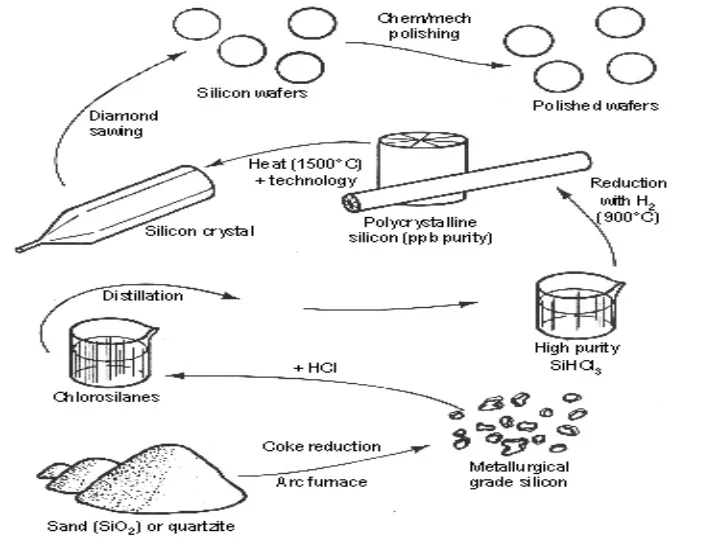
EE-452 13 - 1 Czochralski (CZ) crystal growing Si is purified from SiO2 (sand) by refining, distillation and CVD. It contains < 1 ppb impurities. Pulled crystals contain O ( ~ 1018 EE-452 13 - 2 Plummer cm-3) and C ( ~ 1016 cm-3),


slide-1
SLIDE 1

EE-452 13 - 1

slide-2
SLIDE 2

EE-452 13 - 2

  • Si is purified from SiO2 (sand) by refining, distillation and

CVD.

  • It contains < 1 ppb impurities. Pulled crystals contain O (~1018

cm-3) and C (~1016 cm-3), plus dopants placed in the melt.

Czochralski (CZ) crystal growing

Plummer

slide-3
SLIDE 3

EE-452 13 - 3

Crystal seed Molten polysilicon Heat shield Water jacket Single crystal silicon Quartz crucible Carbon heating element Crystal puller and rotation mechanism

CZ Crystal Puller

Figure 4.10

Plummer

slide-4
SLIDE 4

EE-452 13 - 4

  • All Si wafers come

from “Czochralski” grown crystals.

  • Polysilicon is

melted, then held just below 1417 °C, and a single crystal seed starts the growth.

  • Pull rate, melt

temperature and rotation rate control the growth

lummer

slide-5
SLIDE 5

EE-452 13 - 5

lummer

slide-6
SLIDE 6

EE-452 13 - 6

Silicon Ingot Grown by CZ Method

Photograph courtesy of Kayex Corp., 300 mm Si ingot

Photo 4.1

lummer

slide-7
SLIDE 7

EE-452 13 - 7

slide-8
SLIDE 8

EE-452 13 - 8

An alternative process is the “Float Zone” process which can be used for refining or single crystal growth.

Plummer

slide-9
SLIDE 9

EE-452 13 - 9

Float Zone Crystal Growth

RF Gas inlet (inert) Molten zone Traveling RF coil Polycrystalline rod (silicon) Seed crystal Inert gas out Chuck Chuck

Figure 4.11

lummer

slide-10
SLIDE 10

EE-452 13 - 10

  • In the float zone process, dopants and other impurities are rejected

by the regrowing silicon crystal. Impurities tend to stay in the liquid and refining can be accomplished, especially with multiple passes. (See the Plummer for models of this process)

slide-11
SLIDE 11

EE-452 13 - 11

Flat grind Diameter grind Preparing crystal ingot for grinding

Ingot Diameter Grind

Figure 4.20

Plummer

slide-12
SLIDE 12

EE-452 13 - 12

Internal diameter wafer saw

Internal Diameter Saw

Figure 4.23

Plummer

slide-13
SLIDE 13

EE-452 13 - 13

After crystal pulling, the boule is shaped and cut into wafers which are then polished on one side.

Plummer

slide-14
SLIDE 14

EE-452 13 - 14

Wafer Notch and Laser Scribe

1234567890

Notch

Scribed identification number

Figure 4.22

Plummer

slide-15
SLIDE 15

EE-452 13 - 15

Polished Wafer Edge

Figure 4.24

Plummer

slide-16
SLIDE 16

EE-452 13 - 16

Chemical Etch of Wafer Surface to Remove Sawing Damage

Figure 4.25

slide-17
SLIDE 17

EE-452 13 - 17

Wafer Dimensions & Attributes

Table 4.3

Diameter (mm) Thickness (µm) Area (cm2) Weight (grams/lbs) Weight/25 Wafers (lbs)

150

675 ± 20 176.71 28 / 0.06

1.5 200

725 ± 20 314.16 53.08 / 0.12

3 300

775 ± 20 706.86 127.64 / 0.28

7 400

825 ± 20 1256.64 241.56 / 0.53

13

Plummer

slide-18
SLIDE 18

EE-452 13 - 18

88 die

200-mm wafer

232 die

300-mm wafer

Increase in Number of Chips

  • n Larger Wafer Diameters

(Assume large 1.5 x 1.5 cm microprocessors)

Figure 4.13

Plummer

slide-19
SLIDE 19

EE-452 13 - 19

Wafer Polishing