
SLIDE 1
Conductivity and Semi-Conductors
1
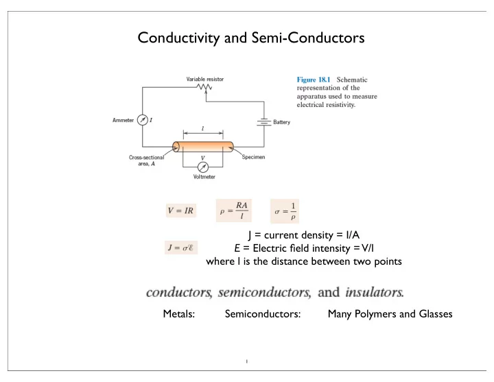
Conductivity and Semi-Conductors J = current density = I/A E = - - PowerPoint PPT Presentation
Conductivity and Semi-Conductors J = current density = I/A E = Electric field intensity = V/l where l is the distance between two points Metals: Semiconductors: Many Polymers and Glasses 1 Electrical Conduction (motion of
1
2
3
4
5
6
7
8
9
10
11
12
13
14
15
Drude Model
16
17
18
19
20
21
22
23
24
25
26
27
28
29
30
31
32
33
34
35
36
37
38
39
Image of a nanoscale heterojunction between iron oxide (Fe3O4 — sphere) and cadmium sulfide (CdS — rod) taken with aTEM. This staggered gap (type II) offset junction was synthesized by Hunter McDaniel and Dr. Moonsub Shim at the University
40
41
42
43
44
45
46
47
48
Energy vs. crystal momentum for a semiconductor with an indirect band gap, showing that an electron cannot shift from the lowest-energy state in the conduction band (green) to the highest-energy state in the valence band (red) without a change in momentum. Here, almost all of the energy comes from a photon (vertical arrow), while almost all of the momentum comes from a phonon (horizontal arrow). Energy vs. crystal momentum for a semiconductor with a direct band gap, showing that an electron can shift from the lowest-energy state in the conduction band (green) to the highest-energy state in the valence band (red) without a change in crystal momentum. Depicted is a transition in which a photon excites an electron from the valence band to the conduction band.
49
50
51
52
53
54
55
56
57
58
59