
SLIDE 1
02/05/2014 1
Slide 4-76
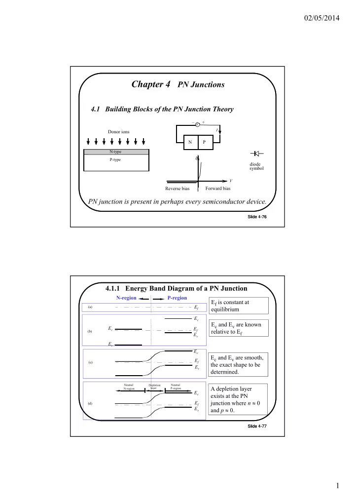
Chapter 4 PN Junctions
PN junction is present in perhaps every semiconductor device.
diode symbol N P
V I
– +
4.1 Building Blocks of the PN Junction Theory
V I
Reverse bias Forward bias Donor ions
N-type P-type Slide 1-76 Slide 4-77
4.1.1 Energy Band Diagram of a PN Junction
A depletion layer exists at the PN junction where n 0 and p 0. Ef is constant at equilibrium Ec and Ev are smooth, the exact shape to be determined. Ec and Ev are known relative to Ef
N-region P-region
(a)
Ef
(c)
Ec Ev Ef
(b)
Ec Ef Ev Ev Ec
(d)
Depletion layer Neutral P-region Neutral N-region
Ec Ev Ef
Slide 1-77