
– 1 – CS:APP3e
Computer Architecture: Logic Design
CSci 2021: Machine Architecture and Organization March 20th-23rd, 2018 Your instructor: Stephen McCamant Based on slides originally by: Randy Bryant and Dave O’Hallaron
– 2 – CS:APP3e
Overview of Logic Design
Fundamental Hardware Requirements
◼ Communication ⚫ How to get values from one place to another ◼ Computation ◼ Storage
Bits are Our Friends
◼ Everything expressed in terms of values 0 and 1 ◼ Communication ⚫ Low or high voltage on wire ◼ Computation ⚫ Compute Boolean functions ◼ Storage ⚫ Store bits of information – 3 – CS:APP3e
Digital Signals
◼ Use voltage thresholds to extract discrete values from
continuous signal
◼ Simplest version: 1-bit signal ⚫ Either high range (1) or low range (0) ⚫ With guard range between them ◼ Not strongly affected by noise or low quality circuit elements ⚫ Can make circuits simple, small, and fast
Voltage Time 1
– 4 – CS:APP3e
Computing with Logic Gates
◼ Outputs are Boolean functions of inputs ◼ Respond continuously to changes in inputs ⚫ With some, small delay
a b
- ut
a b
- ut
a
- ut
- ut = a && b
- ut = a || b
- ut = !a
And Or Not
Voltage Time a b a && b Rising Delay Falling Delay
– 5 – CS:APP3e
Combinational Circuits
Acyclic Network of Logic Gates
◼ Continously responds to changes on primary inputs ◼ Primary outputs become (after some delay) Boolean
functions of primary inputs Acyclic Network Primary Inputs Primary Outputs
– 6 – CS:APP3e
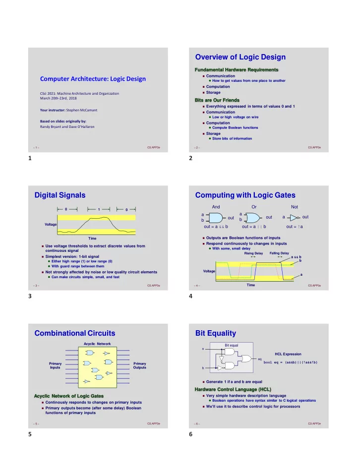
Bit Equality
◼ Generate 1 if a and b are equal
Hardware Control Language (HCL)
◼ Very simple hardware description language ⚫ Boolean operations have syntax similar to C logical operations ◼ We’ll use it to describe control logic for processors
Bit equal a b eq bool eq = (a&&b)||(!a&&!b) HCL Expression