introduction
play

Introduction CPU performance factors Instruction count - PDF document

Morgan Kaufmann Publishers 22 March, 2012 4.1 Introduction Introduction CPU performance factors Instruction count Determined by ISA and compiler CPI and Cycle time Determined by CPU hardware


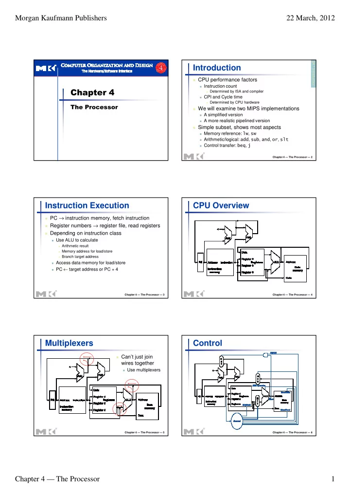
  1. Morgan Kaufmann Publishers 22 March, 2012 §4.1 Introduction Introduction � CPU performance factors � Instruction count ��������� � Determined by ISA and compiler � CPI and Cycle time � Determined by CPU hardware ������������� � We will examine two MIPS implementations � A simplified version � A more realistic pipelined version � Simple subset, shows most aspects � Memory reference: �� , �� � Arithmetic/logical: ��� , ��� , ��� , �� , ��� � Control transfer: ��� , � Chapter 4 — The Processor — 2 Instruction Execution CPU Overview � PC → instruction memory, fetch instruction � Register numbers → register file, read registers � Depending on instruction class � Use ALU to calculate � Arithmetic result � Memory address for load/store � Branch target address � Access data memory for load/store � PC ← target address or PC + 4 Chapter 4 — The Processor — 3 Chapter 4 — The Processor — 4 Multiplexers Control � Can’t just join wires together � Use multiplexers Chapter 4 — The Processor — 5 Chapter 4 — The Processor — 6 Chapter 4 — The Processor 1

  2. Morgan Kaufmann Publishers 22 March, 2012 §4.2 Logic Design Conventions Logic Design Basics Combinational Elements � Information encoded in binary � AND-gate � Adder A � Low voltage = 0, High voltage = 1 + Y � Y = A & B � Y = A + B B � One wire per bit A � Multi-bit data encoded on multi-wire buses Y B � Combinational element � Arithmetic/Logic Unit � Multiplexer � Operate on data � Y = F(A, B) � Y = S ? I1 : I0 � Output is a function of input A I0 M � State (sequential) elements Y ALU Y u I1 x B � Store information S F Chapter 4 — The Processor — 7 Chapter 4 — The Processor — 8 Sequential Elements Sequential Elements � Register: stores data in a circuit � Register with write control � Uses a clock signal to determine when to � Only updates on clock edge when write update the stored value control input is 1 � Edge-triggered: update when Clk changes � Used when stored value is required later from 0 to 1 Clk Clk Write D Q D Q D Write D Clk Clk Q Q Chapter 4 — The Processor — 9 Chapter 4 — The Processor — 10 §4.3 Building a Datapath Clocking Methodology Building a Datapath � Combinational logic transforms data during � Datapath clock cycles � Elements that process data and addresses � Between clock edges in the CPU � Input from state elements, output to state � Registers, ALUs, mux’s, memories, … element � We will build a MIPS datapath � Longest delay determines clock period incrementally � Refining the overview design Chapter 4 — The Processor — 11 Chapter 4 — The Processor — 12 Chapter 4 — The Processor 2

  3. Morgan Kaufmann Publishers 22 March, 2012 Instruction Fetch R-Format Instructions � Read two register operands � Perform arithmetic/logical operation � Write register result Increment by 4 for next instruction 32-bit register Chapter 4 — The Processor — 13 Chapter 4 — The Processor — 14 Load/Store Instructions Branch Instructions � Read register operands � Read register operands � Calculate address using 16-bit offset � Compare operands � Use ALU, but sign-extend offset � Use ALU, subtract and check Zero output � Load: Read memory and update register � Calculate target address � Store: Write register value to memory � Sign-extend displacement � Shift left 2 places (word displacement) � Add to PC + 4 � Already calculated by instruction fetch Chapter 4 — The Processor — 15 Chapter 4 — The Processor — 16 Branch Instructions Composing the Elements � First-cut data path does an instruction in Just one clock cycle re-routes wires � Each datapath element can only do one function at a time � Hence, we need separate instruction and data memories � Use multiplexers where alternate data sources are used for different instructions Sign-bit wire replicated Chapter 4 — The Processor — 17 Chapter 4 — The Processor — 18 Chapter 4 — The Processor 3

  4. Morgan Kaufmann Publishers 22 March, 2012 R-Type/Load/Store Datapath Full Datapath Chapter 4 — The Processor — 19 Chapter 4 — The Processor — 20 §4.4 A Simple Implementation Scheme ALU Control ALU Control � ALU used for � Assume 2-bit ALUOp derived from opcode � Load/Store: F = add � Combinational logic derives ALU control � Branch: F = subtract opcode ALUOp Operation funct ALU function ALU control � R-type: F depends on funct field lw 00 load word XXXXXX add 0010 sw 00 store word XXXXXX add 0010 ALU control Function beq 01 branch equal XXXXXX subtract 0110 0000 AND R-type 10 add 100000 add 0010 0001 OR subtract 100010 subtract 0110 0010 add AND 100100 AND 0000 0110 subtract OR 100101 OR 0001 0111 set-on-less-than set-on-less-than 101010 set-on-less-than 0111 1100 NOR Chapter 4 — The Processor — 21 Chapter 4 — The Processor — 22 The Main Control Unit Datapath With Control � Control signals derived from instruction 0 rs rt rd shamt funct R-type 31:26 25:21 20:16 15:11 10:6 5:0 Load/ 35 or 43 rs rt address Store 31:26 25:21 20:16 15:0 4 rs rt address Branch 31:26 25:21 20:16 15:0 opcode always read, write for sign-extend read except R-type and add for load and load Chapter 4 — The Processor — 23 Chapter 4 — The Processor — 24 Chapter 4 — The Processor 4

  5. Morgan Kaufmann Publishers 22 March, 2012 R-Type Instruction Load Instruction Chapter 4 — The Processor — 25 Chapter 4 — The Processor — 26 Branch-on-Equal Instruction Implementing Jumps 2 address Jump 31:26 25:0 � Jump uses word address � Update PC with concatenation of � Top 4 bits of old PC � 26-bit jump address � 00 � Need an extra control signal decoded from opcode Chapter 4 — The Processor — 27 Chapter 4 — The Processor — 28 Datapath With Jumps Added Performance Issues � Longest delay determines clock period � Critical path: load instruction � Instruction memory → register file → ALU → data memory → register file � Not feasible to vary period for different instructions � Violates design principle � Making the common case fast � We will improve performance by pipelining Chapter 4 — The Processor — 29 Chapter 4 — The Processor — 30 Chapter 4 — The Processor 5

  6. Morgan Kaufmann Publishers 22 March, 2012 §4.5 An Overview of Pipelining Pipelining Analogy MIPS Pipeline � Pipelined laundry: overlapping execution Five stages, one step per stage � � Parallelism improves performance 1. IF: Instruction fetch from memory 2. ID: Instruction decode & register read � Four loads: 3. EX: Execute operation or calculate address � Speedup 4. MEM: Access memory operand = 8/3.5 = 2.3 5. WB: Write result back to register � Non-stop: � Speedup = 2n/0.5n + 1.5 � 4 = number of stages Chapter 4 — The Processor — 31 Chapter 4 — The Processor — 32 Pipeline Performance Pipeline Performance � Assume time for stages is Single-cycle (T c = 800ps) � 100ps for register read or write � 200ps for other stages � Compare pipelined datapath with single-cycle datapath Pipelined (T c = 200ps) Instr Instr fetch Register ALU op Memory Register Total time read access write lw 200ps 100 ps 200ps 200ps 100 ps 800ps sw 200ps 100 ps 200ps 200ps 700ps R-format 200ps 100 ps 200ps 100 ps 600ps beq 200ps 100 ps 200ps 500ps Chapter 4 — The Processor — 33 Chapter 4 — The Processor — 34 Pipeline Speedup Pipelining and ISA Design � MIPS ISA designed for pipelining � If all stages are balanced � All instructions are 32-bits � i.e., all take the same time � Easier to fetch and decode in one cycle � Time between instructions pipelined � c.f. x86: 1- to 17-byte instructions = Time between instructions nonpipelined � Few and regular instruction formats Number of stages � Can decode and read registers in one step � If not balanced, speedup is less � Load/store addressing � Can calculate address in 3 rd stage, access memory � Speedup due to increased throughput in 4 th stage � Latency (time for each instruction) does not � Alignment of memory operands decrease � Memory access takes only one cycle Chapter 4 — The Processor — 35 Chapter 4 — The Processor — 36 Chapter 4 — The Processor 6

Download Presentation
Download Policy: The content available on the website is offered to you 'AS IS' for your personal information and use only. It cannot be commercialized, licensed, or distributed on other websites without prior consent from the author. To download a presentation, simply click this link. If you encounter any difficulties during the download process, it's possible that the publisher has removed the file from their server.

Recommend


More recommend