characterization of multistack cigs cuga in se on mo
play

CHARACTERIZATION OF MULTISTACK CIGS, (CUGA/IN/SE), ON MO COATED SLG - PDF document

18 TH INTERNATIONAL CONFERENCE ON COMPOSITE MATERIALS CHARACTERIZATION OF MULTISTACK CIGS, (CUGA/IN/SE), ON MO COATED SLG BY USING THE IN-LINE SPUTTERING SYSTEM J.S. Park, J.W. Seo , S.W. Park, W.J. Jung, W.N. Kim, C.W. Jeon* School of


  1. 18 TH INTERNATIONAL CONFERENCE ON COMPOSITE MATERIALS CHARACTERIZATION OF MULTISTACK CIGS, (CUGA/IN/SE···), ON MO COATED SLG BY USING THE IN-LINE SPUTTERING SYSTEM J.S. Park, J.W. Seo , S.W. Park, W.J. Jung, W.N. Kim, C.W. Jeon* School of Display and Chem. Eng., Yeungnam University, Gyeongsan 712-749, Korea * Corresponding author(cwjeon@ynu.ac.kr) Keywords : Multi stack CIGS, Se inserted Precursor, Cover glass The conventional selenization process is using Se containing vapor phase to selenize the metal only Abstract precursor, CuInGa, which is called a two step process. During the process, Se is supplied from the The Cu(In,Ga)Se 2 polycrystalline thin films were 
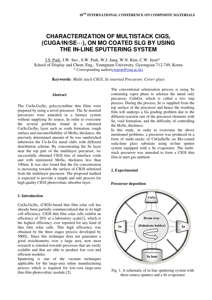
top surface of the precursor and hence the resulting prepared by using a novel precursor. The Se inserted film will undergo a Ga grading problem due to the precursors were annealed in a furnace system different reaction rate of the precursor elements with without supplying Se source. In order to overcome Se, void formation, and the difficulty of controlling the several problems found in a selenized the MoSe 2 thickness. Cu(In,Ga)Se 2 layer such as voids formation, rough In this study, in order to overcome the above surface and uncontrollability of MoSe 2 thickness, the mentioned problems, a precursor was produced in a precisely determined amount of Se was sandwiched form of multi-stacks of CuGa/In/Se on Mo-coated inbetween the Cu-In-Ga metal slabs with different soda-lime glass substrate using in-line sputter distribution scheme. By concentrating the Se layer system equipped with a Se evaporator. The multi- near the top part of the multilayer precursor, we stack precursor was annealed to form a CIGS thin successfully obtained CIGS free of interface voids film in inert gas ambient. and with minimized MoSe 2 thickness less than 100nm. It was also found that the Ga concentration is increasing towards the surface of CIGS selenized 2. Experimental from the multilayer precursor. The proposed method is expected to provide a simple and safe process for high quality CIGS photovoltaic absorber layer. Precursor deposition 1. Introduction Cu(In,Ga)Se 2 (CIGS)-based thin film solar cell has already been partially commercialized due to its high cell efficiency. CIGS thin film solar cells exhibit an efficiency of 20% at a laboratory scale[1], which is the highest efficiency ever reported for any kind of thin film solar cells. This high efficiency was obtained by the three stages process developed by NREL. Since this technique does not guarantee a good stoichiometry over a large area, now most research is oriented towards processes that are easily scalable and that are able to produce low cost and efficient modules. Sputtering is one of the vacuum techniques applicable for the large-area inline manufacturing process which is required for low-cost large-area Fig. 1. A schematic of in-line sputtering system with thin-film photovoltaic module.[2]. three-source sputters and a Se evaporator

  2. CHARACTERIZATION OF MULTISTACK CIGS, (CUGA/IN/SE···), ON MO COATED SLG BY USING THE IN-LINE SPUTTERING SYSTEM The Se inserted precursor films were deposited by Measurements three-source DC magnetron sputtering onto Mo- coated soda-lime glass substrate by using the In-line Both the multi-stack precursors and the CIGS films sputter system as shown in Fig. 1. were analyzed with X-ray diffractometer to check the crystalline properties. A scanning electron The pure In and CuGa(Ga,24wt%) dual targets of 3 microscope (SEM) and energy dispersive inch diameter with 3mm thickness were used. The spectroscopy (EDS) were used to examine the base pressure was 7x10 -7 Torr and working pressure morphology variation and the composition profile. was 5m Torr at room temperature. A drum tray which is used for substrate holder was rotated at 1/3 rpm for fabricating the multi-stacks of CuGa/In/Se. 3 . Results and discussion All four constituent elements (Cu, In, Ga and Se) were deposited by sputtering CuGa and In and evaporating Se. Also, the thickness of precursor with Se was adjusted by DC power at Se boat and amount of it. In order to compare the Ga-pofile, void formation and thickness of MoSe 2 , the position of inserted Se inbetween CIG was intentionally adjusted with a fixed DC power at In and CuGa targets. Selenization The selenization was carried out in a resistive heated quartz furnace. A selenization temperature was 500 ℃ , and the ramp-up speed from room temperature to the target temperature was 22.7 ℃ /min[3]. Once the temperature reached 500 ℃ , the selenization reaction was induced for 5 minutes, then cooling was carried out over 20 minutes. In order to restrain loss of the In, which is known to re-evaporate in the form of volatile In 2 Se compound resulting in copper-rich absorber surface [4,5], the precursor was capped with a sodalime glass during the selenization reaction as shown in Fig 2. The cover glass was easily removed after cooling the sample. Fig. 3. The SEM micrographs showing (a) rough surface morphology and (b) cross-section of CIGS selenized using Se vapor. Figure 3 shows the surface and cross sectional morphology of CIGS obtained by selenizing the metal-only precursor using Se vapor. There are three main features such as interface voids between CIGS and Mo, formation of thick MoSe 2 on top of Mo, and the rough surface. In the two step process, Se must be diffused from top of metal precursor and the metal components should move to the surface, Fig. 2. A schematic of the multilayer precursor and selenization. resulting in the void formation due to the mass transport across the distance as much as the 2

  3. CHARACTERIZATION OF MULTISTACK CIGS, (CUGA/IN/SE···), ON MO COATED SLG BY USING THE IN-LINE SPUTTERING SYSTEM precursor thickness. Unlike the co-evaporated CIGS, a two step selenized CIGS usually has very rough In order to overcome the problems mentioned above surface due to either In agglomeration or volume including voids formation and controllability of expansion during the selenization reaction. MoSe 2 layer, we suggest a novel precursor structure, The normal reaction time using Se vapor is usually where the exact amount of Se required to fully longer than using highly reactive selenide gas such selenize the metallic precursor is inserted inbetween as H 2 Se or diethylselenide (DESe) due to higher CIG layers. binding energy [6]. Therefore, normally the highly The X-ray diffraction pattern and SEM images of excessive Se environment is adopted for promoting the as-deposited (CuGa/In/Se) multilayer precursor selenization rate. Upon the irregular film are shown in Fig. 4. The X-ray diffraction peaks morphology described above, the Se excess indicates the presence of Cu 4 In, free In and CuSe condition makes it difficult to control the thickness phase only. And Fig. 4(b) shows smoother surface of MoSe 2 , which otherwise should be minimized to morphology without any trace of heavily reduce the series resistance of the solar cell. agglomerated In island. Fig. 4(c) shows an exemplary multilayer precursor where the Se layer is evenly distributed across the precursor thickness (the relatively dark line tells the location of Se layer). Fig. 5. The SEM micrographs showing (a) cross- section of CIGS and (b) a surface morphology with cover glass. Fig. 4. X-ray diffraction spectrum of CIGS precursor layer (a) and The SEM micrographs showing (b) a Fig. 5 shows the SEM images of CIGS obtained typical surface morphology and (c) cross-section from annealing the multilayer precursor shown in stacks structure between CuInGa and Se. Fig. 4 at 500 ℃ for 10min in 1atm N 2 environment. 3

  4. CHARACTERIZATION OF MULTISTACK CIGS, (CUGA/IN/SE···), ON MO COATED SLG BY USING THE IN-LINE SPUTTERING SYSTEM Compared to the CIGS shown in Fig. 3, the film surface becomes more uniform due to the minimized mass transport by stacking thin slabs of Se and metals. On the other hand, some of small and large voids were observed from the plan view of the CIGS. The void generation in CIGS synthesized under Se- abundant environment may be attributed to the liquid Cu 2-x Se phase formation promoting grain growth due to the liquid phase assisted diffusion [8]. The voids should be removed, otherwise the device fabricated using the current absorber layer would have very low shunt resistance and hence low fill factor. And the thick MoSe 2 of approximately 500nm, shown in Fig. 3(a), is another aspect of the excess Se. With the intention to resolve the above issues, the total amount of Se is reduced and also the large fraction of Se is concentrated near top surface as shown in Fig. 6(a). Fig. 6. The SEM images; (a) cross-section of multi- layer precursor, (b) cross-section and (c) surface morphology of CIGS annealed with biased Se layer. After annealing of the precursor with the biased Se distribution, it is clear that the surface voids and even the surface morphology of CIGS were considerably improved. Furthermore, MoSe 2 thickness is greatly reduced down to 50~100nm, with which a device performance would not be affected [9]. 4

Download Presentation
Download Policy: The content available on the website is offered to you 'AS IS' for your personal information and use only. It cannot be commercialized, licensed, or distributed on other websites without prior consent from the author. To download a presentation, simply click this link. If you encounter any difficulties during the download process, it's possible that the publisher has removed the file from their server.

Recommend


More recommend