
SLIDE 1
Passivation
- f Si and CIGS surfaces
- Part I: Al2O3 passivation for Si PERx
- Part II: PERC meets CIGS - PercIGS
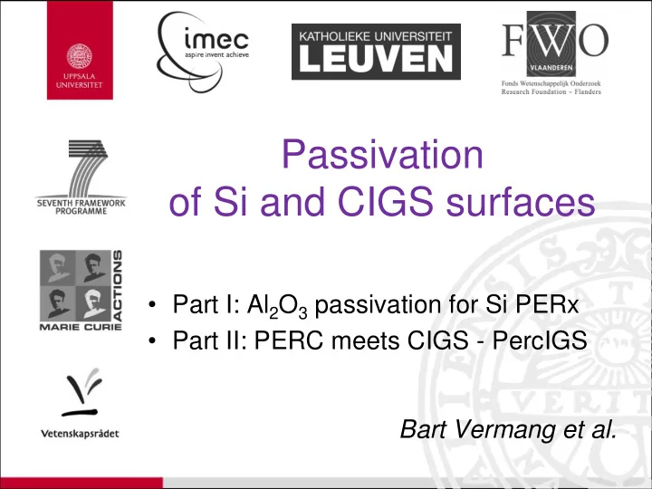
of Si and CIGS surfaces Part I: Al 2 O 3 passivation for Si PERx - - PowerPoint PPT Presentation
Passivation of Si and CIGS surfaces Part I: Al 2 O 3 passivation for Si PERx Part II: PERC meets CIGS - PercIGS Bart Vermang et al. Part I: Al 2 O 3 passivation for Si PERx p- type PERL 20.5 % n-type PERT 21.5 % Rear
(i-)ZnO(:Al) n-CdS p-CIGS Al2O3 pass. layer Soda lime glass Mo Local point contact Local point contact 500 nm
research on wireless communication, biomedical research and long-term brain research
38th IEEE PVSC (2012) DOI: 10.1109/PVSC.2012.6317802
Energy Procedia (2014) DOI: 10.1016/j.egypro.2014.08.041
“temporal” ALD
In-line 1-side depo > 1 nm/s
+ capping + Al metal + firing
EP 2 482 328, TW 2012 50839, US 2012 192943, JP 2012 160732
– VOC = 665 mV; JSC = 38.6 mA/cm2; FF = 79.9 %
Similar technologies: Trina Solar Suntech Canadian Solar Ja Solar Hanwha Solar ...
EP 2 398 044, TW 2012 06857, US 2011 0308603, JP 2012 039088 EP 2 533 305, TW 2013 20188, US 2012 0306058, JP 2012 253356
– Rear passivation of p-type Si PERC =
photo-generated e- from the inverted region via the shunt
– VOC = 677 mV; JSC = 39.1 mA/cm2; FF = 81.3 %
N.-P. Harder, Phys. Status Solidi (a) (2013) DOI: 10.1002/pssa.201329058
My promoter Jef Poortmans and all imec colleagues
– Tunnfilmssolceller / Thin Film Solar Cells
– Fasta Tillståndets Elektronik / Solid State Electronics
Mo sputtering CIGS co-evaporation
CIGS sputtering CZTS sputtering (i-)ZnO(:Al) sputtering CBD CdS ALD (Cd-free) NaF evaporation ARC MgF2 EG evaporation Al/Ni/Al Scribing / lamination Soda lime glass Mo back contact Absorber layer (CIGS) i-ZnO + ZnO:Al Buffer layer (CdS)
Cell and module fabrication Electrical and material characterization
– Cd-free alternative buffers ≥ 20 %
– Focus: northern climate
IEEE J. Photovoltaics (2013) DOI: 10.1109/JPHOTOV.2013.2287769
Uppsala University MSc. Thesis (2014) ISSN: 1650-8300, UPTEC ES14 030
IEEE J. Photovoltaics (2014) in press Thin Solid Films (2014) under review
– Highly recombinative (1x104 cm/s ≤ Sb ≤ 1x106 cm/s) and lowly reflective (Rb < 60 %) – Very comparable to Al BSF in standard Si solar cells
Aluminum
Si
p-type CIGS Mo
BSF Thick absorber layer
passivation layer and micron-sized local point contacts
Passivation layer Micron-sized local point contact Ever thinner wafer thickness
layer and nano-sized local point contacts
(i-)ZnO(:Al) n-CdS p-CIGS Al2O3 pass. layer Soda lime glass Mo Local point contact Local point contact 500 nm Ever thinner absorber layer
– First principle calculations: 35 % reduction in Dit as compared to unpassivated CIGS surface
W.-W. Hsu, Appl. Phys. Lett. (2012) DOI: 10.1063/1.3675849
– Qf < 0 – positive shift in flat-band voltage (VFB) a.f.o. Al2O3 thickness – ∆Qf < 0 – positive shift in VFB after annealing – Reduction in Dit – steeper CV slope after annealing
300 K 50 kHz 300 K 50 kHz as-dep
Rear pass. CIGS solar cell Standard CIGS solar cell
1. Deposit (chemical bath deposition = CBD) a particle-rich CdS layer
2. Deposit the surface passivation layer
3. Remove the CdS nano-particles
Soda Lime Glass (SLG) Mo CdS Pass. layer
Da 1 = 273 nm Da 2 = 270 nm Da 1 = 216 nm Da 2 = 194 nm
1. Deposit Mo NP (formed by a plasma process) on the Mo back contact 2. Deposit the surface passivation layer
SLG Mo Mo NP Pass. layer
(i-)ZnO(:Al) n-CdS p-CIGS Soda lime glass Mo Thin pass. layer Mo NP Mo NP
1. Deposit the surface passivation layer
2. Deposit the resist 3. Open the resist by e-beam litho 4. Etch the passivation layer 5. Remove the resist
SLG Mo Pass. layer Resist
– Well-structured grid
– Al2O3 etching is satisfactory
– Low RS
50 100 150 200 250 300 350 400 450 500
Before PID After PID After recovery
Na intensity (a.u.) CIGS depth (nm)
CdS Al2O3
(a)
p-CIGS n-CdS (i-)ZnO(:Al) Mo Soda lime glass (i-)ZnO(:Al) n-CdS p-CIGS Mo Soda lime glass (i-)ZnO(:Al) n-CdS p-CIGS Mo Soda lime glass
Local contact Local contact Local contact
Approach 1 Approach 2 Approach 3 PERC meets CIGS: PercIGS Introduction of a rear surface passivation layer and nano-sized local contacts Increase in VOC, JSC and FF for rear surface passivated ultra-thin CIGS solar cells compared to (unpassivated) standard ultra- thin CIGS solar cells
J.T. Wätjen
Former: