SLIDE 5 Page 5
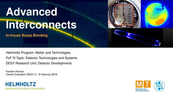
In-house Bump Bonding
CMS Pixel Detector Upgrade Phase I Volume 418 Modules with 6,688 ASICs Rate 6.7 Modules per Week Connectivity Yield ≥ 99.96% best 256 Modules Module Yield Loss
1.2%
3.3%
1% after Repair Bare Module with 66,592 Bumps Connectivity Map of a Class-A Module
: missing Connection
½ Barrel Layer 4 (0.32 m²) Sensor (6.7x1.9 cm²) 16 ASICs 256 x
84% 96% DESY Yield Span Five Production Sites:
Advanced Interconnects | Karsten Hansen
Total Layer 4: KIT / RWTH Aachen DESY / U Hamburg