
SLIDE 1
1
14:332:231 DIGITAL LOGIC DESIGN
Ivan Marsic, Rutgers University Electrical & Computer Engineering Fall 2013
Lecture #9: Combinational Logic Design Practices
2 of 26
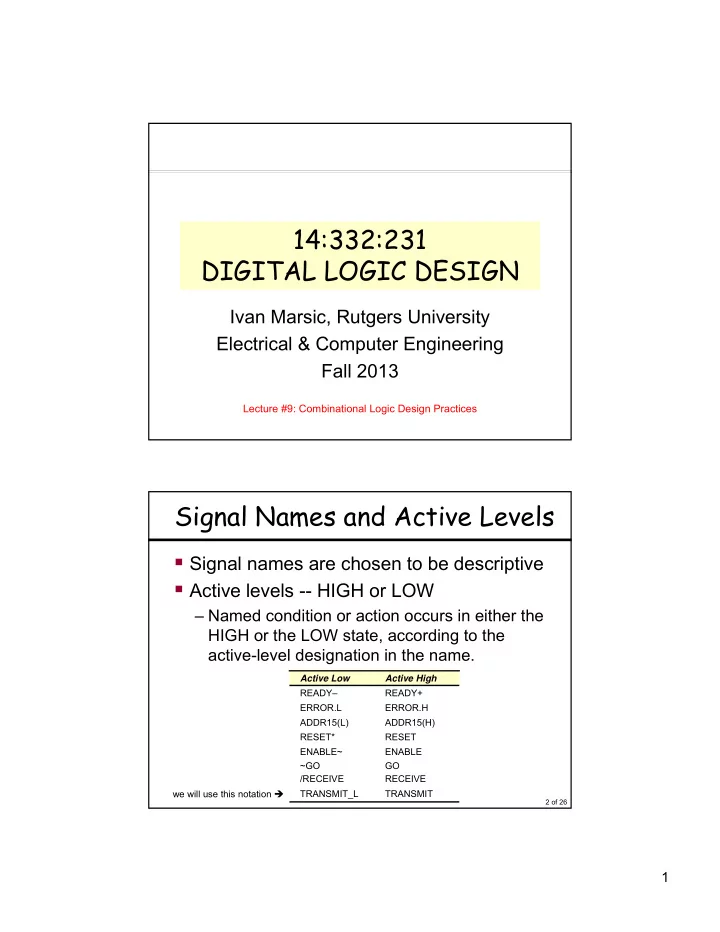
Signal Names and Active Levels
- Signal names are chosen to be descriptive
- Active levels -- HIGH or LOW
– Named condition or action occurs in either the HIGH or the LOW state, according to the active-level designation in the name.
TRANSMIT TRANSMIT_L RECEIVE /RECEIVE GO ~GO ENABLE ENABLE~ RESET RESET* ADDR15(H) ADDR15(L) ERROR.H ERROR.L READY+ READY– Active High Active Low we will use this notation