
SLIDE 1
1
14:332:231 DIGITAL LOGIC DESIGN
Ivan Marsic, Rutgers University Electrical & Computer Engineering Fall 2013
Lecture #12: Multiplexers, Exclusive OR Gates, and Parity Circuits
2 of 31
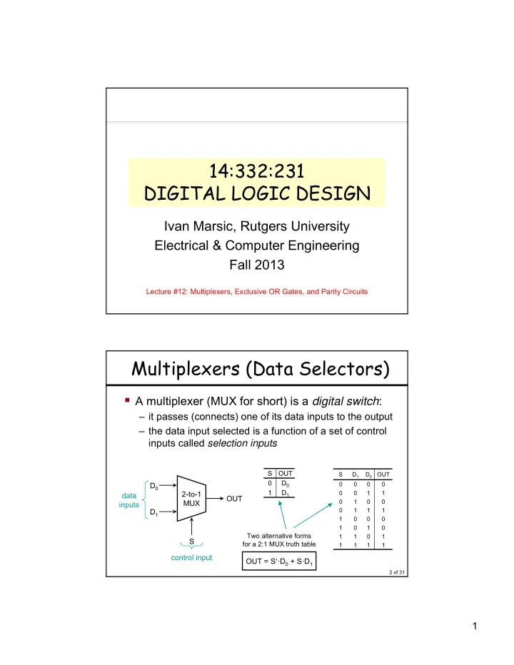
Multiplexers (Data Selectors)
- A multiplexer (MUX for short) is a digital switch:
– it passes (connects) one of its data inputs to the output – the data input selected is a function of a set of control inputs called selection inputs
OUT = S·D0 + S·D1 OUT data inputs control input S 2-to-1 MUX D0 D1
Two alternative forms for a 2:1 MUX truth table D1 1 D0 OUT S
1 1 1 1 1 1 1 1 1 1 1 1 1 1 1 1 OUT D0 D1 S