
SLIDE 1
- L. J. Heyderman
X-Ray Microscopy Techniques
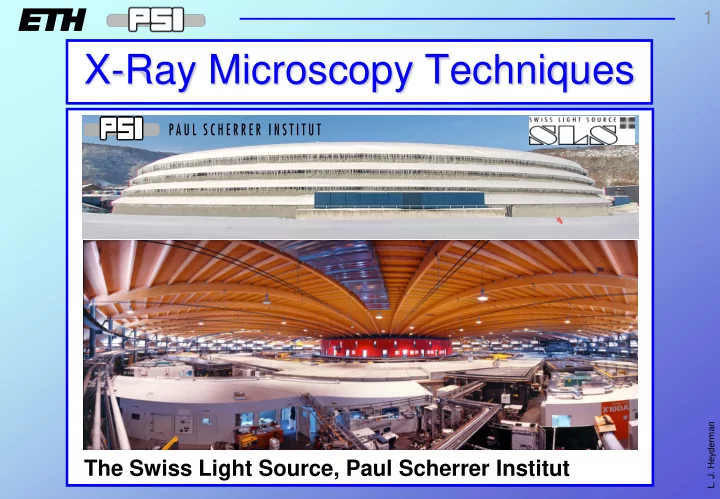
The Swiss Light Source, Paul Scherrer Institut
1
X-Ray Microscopy Techniques L. J. Heyderman The Swiss Light Source, - - PowerPoint PPT Presentation
1 X-Ray Microscopy Techniques L. J. Heyderman The Swiss Light Source, Paul Scherrer Institut 3 The electrons are accelerated close to the speed of light in a linear accelerator and injected into the storage ring Bending magnets or
X-Ray Microscopy Techniques
The Swiss Light Source, Paul Scherrer Institut
1
Reference energy: 2.4 GeV Circumference: 288 m Current: 350 mA (400 mA)
and injected into the storage ring
to bend or wobble through the section and emit light. 3 18 Beamlines
core to the valence band
the valence to the core level gives: Soft x-rays: more Auger es Hard x-rays: more fluorescence
more than just imaging
Evac EF Valence band Core levels Photo electron Auger electron
hν
Fluorescence E
hν
X-ray Absorption Spectroscopy
photon energy Absorption
EF energy
d states s,p states
~ ~
2p 3/2 2p1/2
core level valence band
from core level to valence band
Fermi level
Spectrum: change energy &
X-ray Absorption Spectroscopy
PEEM & TXM
Photon penetration depth 50 nm ~ Electron escape depth 5 nm ~ vacuum sample sample surface
secondary electrons (indirect measure of absorption)
hν Photoemission Electron Microscopy (PEEM) to probe surface / interfaces Transmission X-ray Microscopy (TXM)
X-rays (direct measure of absorption) 7
Slow electrons: mean free path is submono to several monolayers (few nm’s) Surfaces, thin films and interfaces ….consequences for electron optics.
Frithjof Nolting, Swiss Light Source 8
SIM Beamline, Swiss Light Source
The Surface and Interface Microscopy (SIM) Beamline The Photoemission Electron Microscope (PEEM) Close-up of the PEEM 9
Spectromicroscope
L.H. Veneklasen: Ultramicroscopy 36 (1991), 76 Image courtesy of S. Heun (ELETTRA) Elmitec Elektronenmikroskopie GmbH
Clausthal-Zellerfeld, Germany
LEED/LEEM
10
Probe : slow electrons Imaging : high energy electrons (more stable and maintain spatial information) Immersion lens: electrons have before and after the lens different velocity (different wavelength) Cathode lens: Sample is cathode electron microscope is anode Sample “integral part of lens” High Voltage / Ojective Lens 0 eV 20 keV 20 keV
Slow Electrons
Lens Equivalent has two functions: accelerating field due to potential & focussing function
High voltage:
to external magnetic fields
spread and smaller electron beam diameters 12
Two Kinds of Aberrations
Beams parallel away from the lens axis are focused in a slightly different place than beams close to the axis and therefore a blurring of the image. Different wavelengths of light are focused to different positions.
Spherical Chromatic
http://en.wikipedia.org/wiki/Lens_(optics)#Spherical_aberration
Light electrons Glass electrostatic/magnetic lenses
13
Electron energy E Electron energy E+∆E Aperture cuts off transmission of electrons with higher energy
850 900 950 1000 1050 1100 1150 1200 12505 10 15 50 100 150 200 250 300 350 400 energy (eV) 10 25 50 75 100 200 500
Energy distribution is narrowed but transmission (intensity) is reduced. Therefore need to find compromise.
Energy Filter
To remove chromatic aberations:
14
Effect of aperture size on resolution
transmitted electrons and transmission
5 µm 2 mm 12 µm 20 µm 50 µm 0.4 s 100 % 10 s 4 % 4.2 s 9 % 1s 39 %
Aperture diameter Exposure time Transmission
15
Spatial Resolution for Magnetic Imaging
PEEM with X-rays: 50-20 nm spatial resolution Aberration-corrected instruments using an electron mirror: SMART (spectromicroscope for all relevant techniques)
PEEM III
down to a few nm spatial resolution
16
Photoemission Electron Microscope SIM beamline (SLS)
Magnetic lenses
e-
16° analyzer 20 kV
Armin Kleibert Carlos Vaz Ti La Co Fe Elemental Contrast
17
Photoemission Electron Microscope SIM beamline (SLS)
Magnetic lenses
e-
16° analyzer 20 kV
Topographical Contrast
Microfocussing due to distortion
18
Armin Kleibert Carlos Vaz
Photoemission Electron Microscope SIM beamline (SLS)
CCD Magnetic lenses
e-
16° analyzer 20 kV
Element Specific Antiferromagnet Interfaces Time Resolved
19
Armin Kleibert Carlos Vaz
X-Ray Magnetic Circular Dichroism (XMCD)
2p3/2 2p1/2
∆E ~ 1eV ∆l = ±1 ∆s=0
Spin - up Spin - down
EFermi
transition metal
split into spin-up and spin-down with different occupation
polarisation: light mainly excites spin-up/down photoelectrons
resonance intensity reflects number of empty d-band states of a given spin
20
21
Magnetostatic or Stray Field Energy
22
Rectangle, Square, Disk
M HD
23
M HD
Rectangle, Square, Disk
24
M HD
Rectangle, Square, Disk
25
M HD
Rectangle, Square, Disk
26
X-ray Magnetic Circular Dichroism (XMCD)
S
775 780 785 790 795 800 805 L2 L3 Photon energy (eV) TEY (a.u.)
XMCD ~ M cos(M,S) Polarisation: circular plus Polarisation: circular minus 4 µm Magnetic contrast reverses Square Ferromagnetic Element: Landau Domain Pattern
27
M HD
Rectangle, Square, Disk
28
Vortex Onion
Ring
29
Interacting Magnets….. ….with the help of some frogs….!
31
Interacting Magnetic Frogs
32
Ring of Nanomagnets
34
Rings of Nanomagnets
?
35
Three rings Two rings X-ray direction One ring
500 nm
Artificial Spin Ice in PEEM
36
L3a lin. vert L3b lin. vert
X-ray Magnetic Linear Dichroism (XMLD)
E
705 710 715 720 725 730 TEY (a.u.) Photon energy (eV)
720 722 724 726
B A
E
XMLD ~ <M2> cos2(M,E)
2µm
L3 L2
37
circular left or right
symmetric
horizontal
shift 0
linear 0 - 90o
shift π/2 asymmetric
Undulator
Magnetic Structure: changing phase, changes polarisation
38
39
Substrate Permalloy film Cobalt lines
Element specific contrast
Cobalt lines Permalloy film
Coupling of hard and soft magnetic layer:
Co L3 Fe L3 5 µm
700 800 900 Photon Energy (eV) Co Ni Fe
40
Strain and Magnetic Domains
Fe X-ray Linear Dichroism Fe X-ray Magnetic Circular Dichroism
5 µm
Fe XLD: strain domains Fe XMCD: magnetic domains Substrate-induced strain strongly modifies magnetic anisotropy M001 ~ 0
RV Chopdekar et al. PRB (2012)
BaTiO3 CoFe2O4 M010 M100
42
→ Light Stripes → Dark Stripes
A A A A A A A A
Antidot Arrays – Basic Domain Configuration d w p
A A A A
HA
43
Remanent Hysteresis Loop in Antidot Arrays
MOKE
400 Oe
S
2µm
PEEM “Magnetising Holder”
cobalt
Spins to Spins Observe magnetisation reversal in applied magnetic field:
44
a c
MSD
Cobalt Antidot Arrays
b
MSD
2 µm 200 nm
Mengotti et al., JAP (2007) 45
a
200 nm domains in 400 nm GdFeCo nanostructure
¤ ⊗ Switching with a Heat Pulse Only
Switching Experiments
47
a
Thermally Active Switching
48
Iron Nanoparticles Coupled to Cobalt Thin Film
and F. Nolting, PRL (2010)
5-25 nm Fe particles/Co thin Film Noncollinear alignment for particles > 6 nm Spin-spiral magnetic structure determined by magnetic anisotropy energy
49
Time Resolved Imaging
+
H t
100ps
⇒
Why perform time-resolved imaging?
The Horse in Motion 1878, animated in 2006, using photos by Eadward Muybridge, Wikipedia
Are all four feet of a horse off the ground at the same time during a gallop.
Alfred de Dreux (1810 -1860) White horse galloping with two dogs…...
52
15V
Py Al2O3 Au GaAs
HP
x y z
X-Rays: ~1 keV, C+ / C- Laser:
500 nm 0.1 W 10 ps
200 nm 10 nm
IP
Sample Layout
Magnetic Coil + Fast Optical Switch
Pulsed laser illuminates photodiode to give a current pulse. This creates a magnetic field pulse exciting the magnetization.
Magnetic Pump - X-ray Probe
Probe
X-ray pulse
Gate
detector voltage
Pump
Magnetic pulse, laser pulse etc
t ∆t
54
Probe
X-ray pulse
Gate
detector voltage
Pump
Magnetic pulse, laser pulse etc
t ∆t
55
Magnetic Pump - X-ray Probe
Probe
X-ray pulse
Gate
detector voltage
Pump
Magnetic pulse, laser pulse etc
t
56
pump-probe
Magnetic Pump - X-ray Probe
Detect: gated PEEM ∆x ~100nm, ~ 1 ML Pump: stripline / coil Pulse: H < 100 G, 102 ps Probe: X-ray stroboscope ~1keV, ∆t= 70ps
1.04 MHz 500 MHz
e-
Summary
Pump Pulse Sample Combined with Microscope Synchrotron Pulse
16 nanosec gap in bunches, with 70 psec pulse 57
Permalloy (Ni81Fe19) t=30nm Hp~80 Oe
S040906_015Pulse
H P
Py Square: Excitation
58
Permalloy (Ni81Fe19) t=30nm Hp~80 Oe
S040906_015Pulse
H P
Step 1: Coherent rotation ∆t ~ Tprec / 2 ~500ps
Pulse
H M T × =
Step 2: Domain wall motion
Pulse
H M ↑↑
59
Py Square: Excitation
Challenges (limitations):
Summary
60
61
Information on Different Methods
The Analysis of Magnetic Microstructures Magnetic Microscopy of Nanostructures An overview of techniques to image the magnetic structure on the nano-scale
Internet, for example: Techniques to Measure Magnetic Domain Structures, R.J. Celotta, J. Unguris, M.H. Kelley, and D.T. Pierce, Methods in Materials Research (2000)
62
a c
Comparison Between Different Techniques
clean surface,insulators ?
chemical, electronic
63
Further Techniques
64
http://www.fhi-berlin.mpg.de/ http://lma.unizar.es B.-S. Kang et al. J Appl. Phys 98 (2005) 093907
Further Techniques
65
X-rays:
Neutrons: Manke et al. Nat. Comm. (2010)
X-rays: J. Perron et al. PRB (2013) Neutrons: T. Maurer et al. PRB (2014)
67
4th Generation/DLSR (diffraction limited storage ring) → Multibend Achromat (MBA) accelerator lattices → Large increase in brightness → Several soft bend magnets in each storage ring sector replace 2-3 hard bend magnets → smaller horizontal beam dispersion corrected by stronger focusing magnets → elliptical profile replaced by compact and nearly circular profiles, with horizontal spatial & angular widths of source decreased by ∼ factor of 10 relative to existing sources
Soft X-ray Science Opportunities Using Diffraction- Limited Storage Rings, ALS 2014 (Scale → Rectangle Size)
Future Light Sources
Brightness [photons/mm2/mrad2/0.1%BW]
1010 1015 1020 1025 2020 1980 1940 1900 X-ray Tubes 1st Generation 2nd Generation 3rd Generation
15 x 5 mm 500 x 500 µm 500 x 500 µm 15 x 5 mm
Future Challenges
Elem ental Sensitivity
magnetic tunnel junction
Spatial Resolution
exchange length nm µm ns ps fs exchange interactions
Tim e Resolution Peter Fischer, ALS
precession relaxation dynamics (LLG).
repeatable phenomena (stroboscopic pump-probe).
interaction time, spin fluctuation time)
68
69
X-ray Free Electron Lasers
Ultrafast Optical Demagnetisation (100 fs, l=780 nm, 0.2 µJ)
In their conclusions: Ultrafast transport of spin-polarized electrons → Domain size controls time scales & spatial extent. However, exact mechanisms still to be determined…...
a c
Test your understanding……
Magnetic Force Microscopy, Kerr Microscopy & PEEM Which technique:
Can you name any other techniques for imaging magnetic domains?
70