
SLIDE 1
Michael Foerster LEEM-PEEM introduction 19/67/2015
Lucia Aballe Michael Foerster
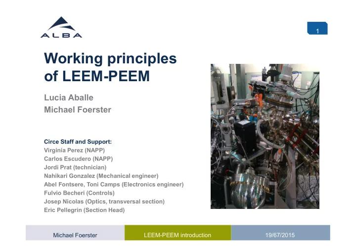
Working principles
- f LEEM-PEEM
Circe Staff and Support: Virginia Perez (NAPP) Carlos Escudero (NAPP) Jordi Prat (technician) Nahikari Gonzalez (Mechanical engineer) Abel Fontsere, Toni Camps (Electronics engineer) Fulvio Becheri (Controls) Josep Nicolas (Optics, transversal section) Eric Pellegrin (Section Head)
1