
SLIDE 1
CBSSS ‘04 Exploring and exploiting novel electronic properties of nanomaterials for computation
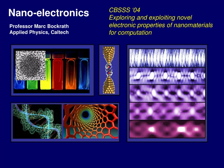
Nano-electronics
Professor Marc Bockrath Applied Physics, Caltech
Nano-electronics Exploring and exploiting novel electronic - - PowerPoint PPT Presentation
CBSSS 04 Nano-electronics Exploring and exploiting novel electronic properties of nanomaterials Professor Marc Bockrath Applied Physics, Caltech for computation Microelectronics The basis for present-day Circuitry patterned on micron
CBSSS ‘04 Exploring and exploiting novel electronic properties of nanomaterials for computation
Professor Marc Bockrath Applied Physics, Caltech
The basis for present-day information technology Circuitry patterned on micron length scale Behavior of microelectronic devices well-described by classical physics, e.g. Ohm’s law
1980 2000 2020 2040 2060 0.1 1 10 100 1000 10000
Year Feature size (nm) For nanometer-scale devices, as quantum mechanics (and other considerations unique to small structures) becomes important, we expect a rich variety of new transport phenomena to be observable
Single-walled nanotubes Nanocrystals Multi-walled nanotubes DNA Cobalt ion + ligands
C Diamond – sp3 Graphite – sp2
1 µm 1 µm
SWNT
Nanotube device geometry
SiO2 Gate
Band structure G vs. Vg E k Metallic SWNT Semiconducting SWNT EF EF Vg G Vg G E k
Low temperature behavior
0.0 1.0 2.0 0.0 2.0
G (µS) Vg (V) T=1.4 K
Energy spacing ∆E between discrete levels determined in principle by solving Schrodinger equation
EF ∆E
States are filled with electrons up to the Fermi level EF in accordance with the Pauli exclusion principle – two electrons per
Energy cost ∆E to add electron to empty
Coulomb repulsion Sets another energy scale U=e2/C Total energy to add electron: U+∆E
U+∆E
Gate voltage can tune the relative position of the energy gap to the Fermi level
Gate Voltage Conductance
20
Vg (arb units) V (mV)
0.00 0.05 0.10
G (µS) Vg (V)
20
20 0.00 0.05 0.10
G (µS) V (mV) Vg (arb units) V (mV)
V (mV) Vg (arb units)
20
Can measure directly U & ∆E
Vg (Arb. units) V (Arb. units) Conductance
2 2.8 2.9 3.0 3.1 3.2 3.3
Gate SiO2 SWNT
2
5
Vg (V) V (mV)
1.6 2.9 dI/dV (e2/h)
5
V (mV)
2
Vg (V)
dI/dV (e2/h) 2.9 3.3
2
5
Vg (V) V (mV)
1.6 2.9 dI/dV (e2/h)
5
V (mV)
2
Vg (V)
dI/dV (e2/h) 2.9 3.3
Vc (meV) L-1 (µm-1) 5 8
L=500 nm L=250 nm
φ /π 2 4 6 Transmission 0.5 1 Incident light time position Overall transmission of light determined by the interference of partially reflected light waves Transmission oscillates as a function of the round trip phase accumulation φ
Incident electron time position
voltage
electrons in the nanotube, resulting in the observed interference pattern
V (mV)
8 Vg (V)
1 2
Vc (meV) L-1 (µm-1) 5 8
Reproduces all the major features of the data Gives energy period of oscillations with no free parameters
Bockrath et al. Nature 2001
10 µm
Micromachine (from Sandia labs) Nanotube bearing motor (Zettl group, Nature ‘03) Nnaotube nanomechanical memory (Lieber group, Science ‘00) Mechanical computing paradigm e.g., Babbage ‘analytical engine’
MWNT MWNT
100 200 250
Time (s) I (µA)
From H.-Y. Chiu Related work, P. Collins, J. Cumings et al.
4
15
V (V) I (µA)
From V. Deshpande
Bearing extended
100 nm
Chemical synthesis of individual molecules allows construction
atomic precision
Liang et al. Nature (’02)
Individual divanadium molecule transistors studied using electromigration- induced break-junction technique
Park et al., APL (’98)
events leads to a narrow Kondo resonance near the Fermi energy of the leads.
indicates spin degeneracy. Schematic Diagram (S=1/2)
Kondo effect in GaAs quantum dots: Goldhaber-Gordon et al. Nature (’98), Cronenwett et al. Science (’98)
Kondo temperature exponentially decaying in ε, in accordance with theoretical predictions (e.g. Haldane et al.)
DNA similar in diameter to nanotubes Its recognition capabilities may enable self-assembly of nanoelectronic circuits
But........
YES
Fink & Schonenberger Nature (1999) Kasumov et al. Science (2001) ETC. Porath et al., Nature (2000) de Pablo et al., PRL (2000) ETC.
NO
Tip applies potential so as to induce local charge density Presence of absence of charge determined by monitoring the cantilever resonant frequency
Charge motion takes a characteristic time equal to the RC time constant of the wire This time constant is ~10-10 s for a 1MΩ Tip scans over wire in characteristic time ~10-3 s
AFM tip Current
10 µm long wire
L (µm) 5 10 G0 (Ω-1 – cm) 10-22 10-16 10-10
Can detect extremely low conductivity wires!
Scanned Con Image ductance Topographic Image λ-DNA Nanotube
0.1 µm No signal from the λ-DNA in the scanned Conductance image
Bockrath et al. Nanoletters (’02)
Nanowire Crossbar array – potential for high integration density
Problem: Voltage applied to one wire acts on all the crossing wires in parallel
Crossed Si nanowires, one used as a gate electrode, the other as a MOSFET channel With Lieber group Zhong et al., Science (2003)
Untreated junction Treated with tetraethyl ammonium chloride
Junctions can be selectively treated to enable independently controllable function
Design a system of logic gates based on single-electron transistors Example: NOT gate
From K. Likharev
Nanotube Transport Scanned Conductance Microscopy Nina Markovic Adam Shepard Leonid Gurevich Leo Kouwenhoven Minshaw Wu Lydia Sohn Wenjie Liang Hongkun Park Michael Tinkham Jason Hafner Charles Lieber Nanotube Relay Vikram Deshpande Hsin-Ying Chiu Si nanowire wire decoder Zhaohui Zhong Deli Wang Yi Cui Charles M. Lieber Molecule SET Wenjie Liang Matthew Shores Jeffrey Long Hongkun Park