verilog 1 fundamentals
play

Verilog 1 - Fundamentals FA FA FA FA module adder( input [3:0] - PowerPoint PPT Presentation

Verilog 1 - Fundamentals FA FA FA FA module adder( input [3:0] A, B, output cout, output [3:0] S ); wire c0, c1, c2; FA fa0( A[0], B[0], 1b0, c0, S[0] ); FA fa1( A[1], B[1], c0, c1, S[1] ); FA fa2( A[2], B[2], c1, c2,


  1. Verilog 1 - Fundamentals FA FA FA FA module adder( input [3:0] A, B, output cout, output [3:0] S ); wire c0, c1, c2; FA fa0( A[0], B[0], 1’b0, c0, S[0] ); FA fa1( A[1], B[1], c0, c1, S[1] ); FA fa2( A[2], B[2], c1, c2, S[2] ); FA fa3( A[3], B[3], c2, cout, S[3] ); endmodule 6.375 Complex Digital Systems Arvind
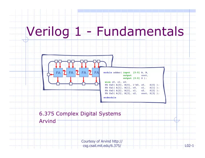
 Courtesy of Arvind http:// csg.csail.mit.edu/6.375/ L02-1

  2. Verilog Fundamentals History of hardware design languages Data types Structural Verilog Simple behaviors FA FA FA FA module adder( input [3:0] A, B, output cout, output [3:0] S ); wire c0, c1, c2; FA fa0( A[0], B[0], 1’b0, c0, S[0] ); FA fa1( A[1], B[1], c0, c1, S[1] ); FA fa2( A[2], B[2], c1, c2, S[2] ); FA fa3( A[3], B[3], c2, cout, S[3] ); endmodule Courtesy of Arvind http:// csg.csail.mit.edu/6.375/ L02-2

  3. Originally designers used breadboards for prototyping Number of Gates in Design 10 7 Solderless Breadboard 10 6 10 5 tangentsoft.net/elec/breadboard.html No symbolic 10 4 execution or testing 10 3 10 2 Printed circuit board 10 home.cogeco.ca Courtesy of Arvind http:// csg.csail.mit.edu/6.375/ L02-3

  4. HDLs enabled logic level simulation and testing Number of Gates Gate Level in Design Description 10 7 Simulate Test 10 6 Results Manual 10 5 10 4 10 3 10 2 HDL = Hardware Description Language 10 Courtesy of Arvind http:// csg.csail.mit.edu/6.375/ L02-4

  5. Designers began to use HDLs for higher level design Number of Gates Simulate Behavioral Test in Design Algorithm Results 10 7 Simulate 10 6 Test Register Results Transfer Level 10 5 Simulate 10 4 Test Gate Level Results 10 3 10 2 Manual 10 Courtesy of Arvind http:// csg.csail.mit.edu/6.375/ L02-5

  6. HDLs led to tools for automatic translation Number of Gates Simulate Behavioral Test in Design Algorithm Results 10 7 Manual Simulate 10 6 Test Register Results Transfer Level 10 5 Logic Synthesis Simulate 10 4 Test Gate Level Results 10 3 Auto Place + Route 10 2 HDLs: Verilog, VHDL… Tools: Spice, ModelSim, 10 DesignCompiler, … Courtesy of Arvind http:// csg.csail.mit.edu/6.375/ L02-6

  7. Raising the abstraction further … Number of Gates Simulate Guarded Atomic Test in Design Actions Results 10 7 GAA Compiler Simulate 10 6 Test Register Results Transfer Level 10 5 Logic Synthesis Simulate 10 4 Test Gate Level Results 10 3 Auto Place + Route 10 2 10 Courtesy of Arvind http:// csg.csail.mit.edu/6.375/ L02-7

  8. The current situation Behavioral RTL C, C++, MATLAB SystemC Verilog, VHDL, SystemVerilog Structural RTL Register Verilog, VHDL, Transfer Level SystemVerilog Logic Synthesis Simulators and other tools Gate Level are available at all levels but not compilers from the behavioral level to RTL Courtesy of Arvind http:// csg.csail.mit.edu/6.375/ L02-8

  9. Verilog Fundamentals History of hardware design languages Data types Structural Verilog Simple behaviors FA FA FA FA module adder( input [3:0] A, B, output cout, output [3:0] S ); wire c0, c1, c2; FA fa0( A[0], B[0], 1’b0, c0, S[0] ); FA fa1( A[1], B[1], c0, c1, S[1] ); FA fa2( A[2], B[2], c1, c2, S[2] ); FA fa3( A[3], B[3], c2, cout, S[3] ); endmodule Courtesy of Arvind http:// csg.csail.mit.edu/6.375/ L02-9

  10. Bit-vector is the only data type in Verilog A bit can take on one of four values Value Meaning 0 Logic zero 1 Logic one X Unknown logic value Z High impedance, floating An X bit might be a 0, 1, Z, or in transition. We can set bits to be X in situations where we don’t care what the value is. This can help catch bugs and improve synthesis quality. Courtesy of Arvind http:// csg.csail.mit.edu/6.375/ L02-10

  11. “wire” is used to denote a hardware net wire [15:0] instruction; Absolutely no type wire [15:0] memory_req; safety when wire [ 7:0] small_net; connecting nets! ? memory_req instruction instruction small_net Courtesy of Arvind http:// csg.csail.mit.edu/6.375/ L02-11

  12. Bit literals Binary literals 4’b10_11  8’b0000_0000  8’b0xx0_1xx1 Hexadecimal literals Underscores  32’h0a34_def1 are ignored  16’haxxx Base format (d,b,o,h) ‏ Decimal literals Decimal number  32’d42 representing size in bits We’ll learn how to actually assign literals to nets a little later Courtesy of Arvind http:// csg.csail.mit.edu/6.375/ L02-12

  13. Verilog Fundamentals History of hardware design languages Data types Structural Verilog Simple behaviors FA FA FA FA module adder( input [3:0] A, B, output cout, output [3:0] S ); wire c0, c1, c2; FA fa0( A[0], B[0], 1’b0, c0, S[0] ); FA fa1( A[1], B[1], c0, c1, S[1] ); FA fa2( A[2], B[2], c1, c2, S[2] ); FA fa3( A[3], B[3], c2, cout, S[3] ); endmodule Courtesy of Arvind http:// csg.csail.mit.edu/6.375/ L02-13

  14. Our Verilog Subset Verilog is a big language with many features not concerned with synthesizing hardware. The code you write for your processor should only contain the languages structures discussed in these slides. Anything else is not synthesizable, although it will simulate fine. Courtesy of Arvind http:// csg.csail.mit.edu/6.375/ L02-14

  15. A Verilog module has a name and a port list A B module adder( A, B, cout, sum ); 4 4 input [3:0] A; input [3:0] B; output cout; adder output [3:0] sum; // HDL modeling of 4 // adder functionality endmodule cout sum Note the semicolon at the end of the port Ports must have a list! direction (or be bidirectional) and a bitwidth Courtesy of Arvind http:// csg.csail.mit.edu/6.375/ L02-15

  16. Alternate syntax A B Traditional Verilog-1995 Syntax 4 4 module adder( A, B, cout, sum ); input [3:0] A; input [3:0] B; adder output cout; output [3:0] sum; 4 ANSI C Style Verilog-2001 Syntax cout sum module adder( input [3:0] A, input [3:0] B, output cout, output [3:0] sum ); Courtesy of Arvind http:// csg.csail.mit.edu/6.375/ L02-16

  17. A module can instantiate other modules A B adder FA FA FA FA cout S a b cin module adder( input [3:0] A, B, cout FA output cout, output [3:0] S ); c wire c0, c1, c2; module FA( input a, b, cin FA fa0( ... ); output cout, sum ); FA fa1( ... ); // HDL modeling of 1 bit FA fa2( ... ); // full adder functionality FA fa3( ... ); endmodule endmodule Courtesy of Arvind http:// csg.csail.mit.edu/6.375/ L02-17

  18. Connecting modules A B adder FA FA FA FA cout S module adder( input [3:0] A, B, output cout, output [3:0] S ); wire c0, c1, c2; FA fa0( A[0], B[0], 1’b0, c0, S[0] ); FA fa1( A[1], B[1], c0, c1, S[1] ); FA fa2( A[2], B[2], c1, c2, S[2] ); FA fa3( A[3], B[3], c2, cout, S[3] ); Carry Chain endmodule Courtesy of Arvind http:// csg.csail.mit.edu/6.375/ L02-18

  19. Alternative syntax Connecting ports by ordered list FA fa0( A[0], B[0], 1’b0, c0, S[0] ); Connecting ports by name (compact) FA fa0( .a(A[0]), .b(B[0]), .cin(1’b0), .cout(c0), .sum(S[0]) ); Argument order does not matter when ports are connected by name FA fa0 ( .a (A[0]), Connecting ports by name .cin (1’b0), yields clearer and less .b (B[0]), buggy code. .cout (c0), .sum (S[0]) ); Courtesy of Arvind http:// csg.csail.mit.edu/6.375/ L02-19

  20. Verilog Fundamentals History of hardware design languages Data types Structural Verilog Simple behaviors FA FA FA FA module adder( input [3:0] A, B, output cout, output [3:0] S ); wire c0, c1, c2; FA fa0( A[0], B[0], 1’b0, c0, S[0] ); FA fa1( A[1], B[1], c0, c1, S[1] ); FA fa2( A[2], B[2], c1, c2, S[2] ); FA fa3( A[3], B[3], c2, cout, S[3] ); endmodule Courtesy of Arvind http:// csg.csail.mit.edu/6.375/ L02-20

  21. A module’s behavior can be described in many different ways but it should not matter from outside Example: mux4 Courtesy of Arvind http:// csg.csail.mit.edu/6.375/ L02-21

  22. mux4: Gate-level structural Verilog module mux4(input a,b,c,d, input [1:0] sel, output out); wire [1:0] sel_b; b d a c sel[1] sel[0] not not0( sel_b[0], sel[0] ); not not1( sel_b[1], sel[1] ); wire n0, n1, n2, n3; and and0( n0, c, sel[1] ); and and1( n1, a, sel_b[1] ); and and2( n2, d, sel[1] ); and and3( n3, b, sel_b[1] ); wire x0, x1; nor nor0( x0, n0, n1 ); nor nor1( x1, n2, n3 ); wire y0, y1; or or0( y0, x0, sel[0] ); or or1( y1, x1, sel_b[0] ); nand nand0( out, y0, y1 ); out Courtesy of Arvind http:// endmodule csg.csail.mit.edu/6.375/ L02-22

  23. mux4: Using continuous assignments Language defined module mux4( input a, b, c, d operators input [1:0] sel, output out ); wire out, t0, t1; assign out = ~( (t0 | sel[0]) & (t1 | ~sel[0]) ); assign t1 = ~( (sel[1] & d) | (~sel[1] & b) ); assign t0 = ~( (sel[1] & c) | (~sel[1] & a) ); endmodule The order of these continuous assignment statements does not matter. They essentially happen in parallel! Courtesy of Arvind http:// csg.csail.mit.edu/6.375/ L02-23

  24. mux4: Behavioral style // Four input multiplexer module mux4( input a, b, c, d input [1:0] sel, output out ); assign out = ( sel == 0 ) ? a : ( sel == 1 ) ? b : ( sel == 2 ) ? c : ( sel == 3 ) ? d : 1’bx; endmodule If input is undefined we want to propagate that information. Courtesy of Arvind http:// csg.csail.mit.edu/6.375/ L02-24

Download Presentation
Download Policy: The content available on the website is offered to you 'AS IS' for your personal information and use only. It cannot be commercialized, licensed, or distributed on other websites without prior consent from the author. To download a presentation, simply click this link. If you encounter any difficulties during the download process, it's possible that the publisher has removed the file from their server.

Recommend


More recommend