
SLIDE 1 K Y O T O U N I V E R S I T Y F O U N D E D 1 8 9 7
KYOTO JAPAN
Kyoto Univ. 第28回無機材料に関する最近の研究成果発表会, 2011. 1. 24, 東海大学校友会館
U N I V O E T R O S Y I T K Y Kyoto Univ. 28 - - PowerPoint PPT Presentation
U N I V O E T R O S Y I T K Y Kyoto Univ. 28 , 2011. 1. 24, F KYOTO JAPAN 7 O 9 U 8 1 N D E D Progress
Kyoto Univ. 第28回無機材料に関する最近の研究成果発表会, 2011. 1. 24, 東海大学校友会館
Kyoto Univ. 第28回無機材料に関する最近の研究成果発表会, 2011. 1. 24, 東海大学校友会館
Au SiO2 SiO2
Au, Ag nanorod arrays LR-WG polarizers
SERS & PC-SERS
prolate Ag nanoparticles by dynamic oblique deposition," Jpn. J. Appl. Phys. Part 2 44 (1-7), L193-L195 (2005).
nanorods for surface-enhanced Raman spectroscopy," Appl. Phys. Lett. 88 (20), 203121 (2006).
absorptive interference overlayers," Nanotechnology 21 (17), 175604 (2010).
Local plasmon resonator for SERS
plasmons by using Ag nanorods/structured dielectric/mirror sandwiches," Journal of Nanophotonics 3 (1), 031502 (2009).
for micro-fluid?
Wavelength selective IR emitters?
Polarizer
Spatiotemporal nanoheaters
http://www.nidek.co.jp/
Kyoto Univ. 第28回無機材料に関する最近の研究成果発表会, 2011. 1. 24, 東海大学校友会館
Kyoto Univ. 第28回無機材料に関する最近の研究成果発表会, 2011. 1. 24, 東海大学校友会館
[1]
Continuous, Phase-Modulated, and Pulsed Light with Quantitation of Blood and Blood Oxygenation," Annals of the New York Academy of Sciences 838, 29-45 (1998).
Kyoto Univ. 第28回無機材料に関する最近の研究成果発表会, 2011. 1. 24, 東海大学校友会館
top down bottom up random
Orendorff et al., Anal. Chem. 77, (2005) 3261.
Random aggregates of nanorods
Liao et al., Chem. Phys. Lett. 82 (1981) 355.
Evaporated on lithographic template.
Martínes et al., Phys. Rev. B 35 (1987) 9481.
Obliquely deposited columns.
EB lithographic arrays.
side by side
Local field can be significantly enhanced at the end of nanorod. Further enhancement is expected for in-line alignment. Low cost Expensive
Kyoto Univ. 第28回無機材料に関する最近の研究成果発表会, 2011. 1. 24, 東海大学校友会館
Kyoto Univ. 第28回無機材料に関する最近の研究成果発表会, 2011. 1. 24, 東海大学校友会館
Nucleation Self-shadowing Columnar growth
deposited thin films are the self-shadowing effects and the limited mobility of the deposited atoms.
films shadow unoccupied sites from the direct sticking of incident atoms.
beam.
Kyoto Univ. 第28回無機材料に関する最近の研究成果発表会, 2011. 1. 24, 東海大学校友会館
deposition angle;
αSiO2
substrate
SiO2
① Preparation of SiO2 template
αSiO2 → 79˚ dSiO2 → 0 — 500 nm
Substrate is set at oblique angle and rotated by 180˚ with each deposition of 10 nm thick.
(Serial bideposition[SBD])
Substrate: Ordinary flat glass
Kyoto Univ. 第28回無機材料に関する最近の研究成果発表会, 2011. 1. 24, 東海大学校友会館
αAg Ag
deposition angle: αAg
② Oblique deposition of Ag (or Au)
thickness of Au, Ag; dAu, Ag
αAu, Ag → 73˚ dAu, Ag→ 125 nm
Au, Ag
Kyoto Univ. 第28回無機材料に関する最近の研究成果発表会, 2011. 1. 24, 東海大学校友会館
SEM of Au nanorods. Absorbance spectra. SERS spectra of 4,4’-bpy solutions measured on Au
Ag nanordos
4,4’-bipyridine 1 mM solution
[1]
Surface-Enhanced Raman Spectroscopy," Analytical Sciences 23 (7), 829-833 (2007).
Kyoto Univ. 第28回無機材料に関する最近の研究成果発表会, 2011. 1. 24, 東海大学校友会館
1014 cm-1近傍のピーク強度の 濃度依存
Kyoto Univ. 第28回無機材料に関する最近の研究成果発表会, 2011. 1. 24, 東海大学校友会館
ページ 1/2 https://www.nidek.co.jp/products/coating_others/sers.html
Kyoto Univ. 第28回無機材料に関する最近の研究成果発表会, 2011. 1. 24, 東海大学校友会館
Au nanorods
rather stable and reproducible.
SERS is measured without analyte.
temporary unstable.
SERS spectra of air Unidentified peaks are due to the contaminations on the surface of Au
serious problems for the highly sensitive Au nanorod arrays.
Kyoto Univ. 第28回無機材料に関する最近の研究成果発表会, 2011. 1. 24, 東海大学校友会館
Kyoto Univ. 第28回無機材料に関する最近の研究成果発表会, 2011. 1. 24, 東海大学校友会館
Vacuum equipment is required beside Raman Microscope
[1] R. J. Walsh and G. Chumanov, "Silver Coated Porous Alumina as a New Substrate for Surface-Enhanced Raman Scattering," App. Spectroscopy 55 (12), 1695-1700 (2001).
Kyoto Univ. 第28回無機材料に関する最近の研究成果発表会, 2011. 1. 24, 東海大学校友会館
TiO2, Au TiO2 cross section surface TiO2, Au TiO2
Kyoto Univ. 第28回無機材料に関する最近の研究成果発表会, 2011. 1. 24, 東海大学校友会館
Au nanorods TiO2 template
Au/TiO2 dAu=5 nm, αAu=83°
TiO2 glass
UV LED MB solution
Kyoto Univ. 第28回無機材料に関する最近の研究成果発表会, 2011. 1. 24, 東海大学校友会館
dAu=5 nm, αAu=83° dAu=10 nm, αAu=73°
100 200 300 400 500 600 700 800 500 1000 1500 2000 intensity (a.u.) Raman shift (cm-1) 200 400 600 800 1000 1200 500 1000 1500 2000 intensity (a.u.) Raman shift (cm-1)
Au nanorods TiO2 template
4,4’-bipyridine solution
TiO2 TiO2 4,4’-BiPy 4,4’-BiPy
[1] P. J. Huang, H. Chang, C. T. Yeh, and C. W. Tsai, "Phase transformation of TiO2 monitored by Thermo-Raman spectroscopy with TGA/DTA," Thermochimica Acta 297 (1-2), 85-92 (1997).
515 640 515 640
Kyoto Univ. 第28回無機材料に関する最近の研究成果発表会, 2011. 1. 24, 東海大学校友会館 100 200 300 400 500 600 700 800 500 1000 1500 2000 intensity (a.u.) Raman shift (cm-1) 0 min 5 min 10 min 15 min
Au nanorods TiO2 template
UV LED
TiO2 SiO2
Kyoto Univ. 第28回無機材料に関する最近の研究成果発表会, 2011. 1. 24, 東海大学校友会館
Further enhancement of SERS is expected by improvement of coupling of local plasmon with photon.
100 300 300 300 500 73 73 73 85 73
tAu = 10 nm
Kyoto Univ. 第28回無機材料に関する最近の研究成果発表会, 2011. 1. 24, 東海大学校友会館
Au SiO2 SiO2
Au, Ag nanorod arrays LR-WG polarizers
SERS & PC-SERS
prolate Ag nanoparticles by dynamic oblique deposition," Jpn. J. Appl. Phys. Part 2 44 (1-7), L193-L195 (2005).
nanorods for surface-enhanced Raman spectroscopy," Appl. Phys. Lett. 88 (20), 203121 (2006).
absorptive interference overlayers," Nanotechnology 21 (17), 175604 (2010).
Local plasmon resonator for SERS
plasmons by using Ag nanorods/structured dielectric/mirror sandwiches," Journal of Nanophotonics 3 (1), 031502 (2009).
for micro-fluid?
Wavelength selective IR emitters?
Polarizer
Spatiotemporal nanoheaters
http://www.nidek.co.jp/
Kyoto Univ. 第28回無機材料に関する最近の研究成果発表会, 2011. 1. 24, 東海大学校友会館
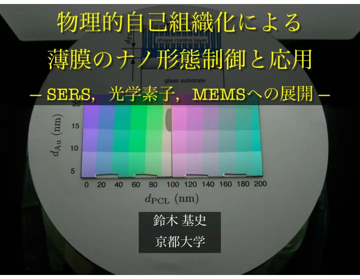
Ag mirror (200 nm) glass substrate stepped phase control layer Au nanorods shape control layer (500 nm)
Flat Ag film deposited at α=0˚ SiO2 film deposited at α=0˚: flat but stepped by moving a shutter. 0 − 200 nm. SiO2 film serial-bideposited at α=79˚. Au deposited at α=73˚, average thickness=10 nm.
enhance the coupling of light to the local plasmon. ≈ To minimize reflectance of Au NRA/SCL/PCL/Ag mirror.
thicknesses were realized.
Kyoto Univ. 第28回無機材料に関する最近の研究成果発表会, 2011. 1. 24, 東海大学校友会館
Ag mirror (200 nm) glass substrate stepped phase control layer Au nanorods shape control layer (500 nm)
Kyoto Univ. 第28回無機材料に関する最近の研究成果発表会, 2011. 1. 24, 東海大学校友会館
Morphology & spectra of local plasmon resonators
(a) (b) glass subst. Ag mirror PCL (SiO2) SCL (SiO2) A u N R A
SiO2 SiO2 Au
SiO2 SiO2 Au s'-polarized p'-polarized
thickness of the phase control layer.
500 nm
phase control layer Ag mirror (200 nm) Au nanorods shape control layer
dP
glass substrate
abscissa: photon energy
dAu = 10 nm
Colors: − log10 R yellow→small R & large absorption purple →large R & small absorption
Kyoto Univ. 第28回無機材料に関する最近の研究成果発表会, 2011. 1. 24, 東海大学校友会館
(b)
1 2 500 1000 1500 intensity (a.u.) Raman shift (cm-1) dP=75 nm dP=150 nm
(a)
Selected SERS spectra and the SERS spectra as a function of dP.
AR condition.
NRA without mirror.
expected.
phase control layer Ag mirror (200 nm) Au nanorods shape control layer
dP
glass substrate
λ=785 nm
Ag nanordos
4,4’-bipyridine (model analyte) 1 mM solution Au NRA
Kyoto Univ. 第28回無機材料に関する最近の研究成果発表会, 2011. 1. 24, 東海大学校友会館
Kyoto Univ. 第28回無機材料に関する最近の研究成果発表会, 2011. 1. 24, 東海大学校友会館
Au SiO2 SiO2
Au, Ag nanorod arrays LR-WG polarizers
SERS & PC-SERS
prolate Ag nanoparticles by dynamic oblique deposition," Jpn. J. Appl. Phys. Part 2 44 (1-7), L193-L195 (2005).
nanorods for surface-enhanced Raman spectroscopy," Appl. Phys. Lett. 88 (20), 203121 (2006).
absorptive interference overlayers," Nanotechnology 21 (17), 175604 (2010).
Local plasmon resonator for SERS
plasmons by using Ag nanorods/structured dielectric/mirror sandwiches," Journal of Nanophotonics 3 (1), 031502 (2009).
for micro-fluid?
Wavelength selective IR emitters?
Polarizer
http://www.nidek.co.jp/
Spatiotemporal nanoheaters
Kyoto Univ. 第28回無機材料に関する最近の研究成果発表会, 2011. 1. 24, 東海大学校友会館
20 40 60 80 100 12.6 9.1 10.3 11.5
50mm
dP
phase control layer (SiO2) Ag mirror
shape control layer (SiO2)
substrate Au nanorods
Kyoto Univ. 第28回無機材料に関する最近の研究成果発表会, 2011. 1. 24, 東海大学校友会館
phase control layer Ag mirror (200 nm) Au nanorods
shape control layer (400 nm)
dP
glass substrate
Kyoto Univ. 第28回無機材料に関する最近の研究成果発表会, 2011. 1. 24, 東海大学校友会館
fit with only one parameter of Q.
phase control layer Ag mirror (200 nm) Au nanorods
shape control layer (400 nm)
dP
glass substrate
T0 Q(T-T0)
heating
efficiency is controlled by thickness of PCL. absorber reflector
Kyoto Univ. 第28回無機材料に関する最近の研究成果発表会, 2011. 1. 24, 東海大学校友会館
0.5 μm∼100 mm Low thermal conductance
High thermal conductance
dP
phase control layer (SiO2) Ag mirror
shape control layer (SiO2)
substrate Au nanorods
Kyoto Univ. 第28回無機材料に関する最近の研究成果発表会, 2011. 1. 24, 東海大学校友会館
Kyoto Univ. 第28回無機材料に関する最近の研究成果発表会, 2011. 1. 24, 東海大学校友会館
[1]
polarizers in modern LCOS light-engine configurations," Journal
polymer polarizer WG polarizers Recycling light
Kyoto Univ. 第28回無機材料に関する最近の研究成果発表会, 2011. 1. 24, 東海大学校友会館
& dry etching. → Normal deposition of gap layer (SiO2).
covered with the gap layer of SiO2.
Al FeSi2 SiO2
(a) (b) (c)
FeSi
2
Al WG: width; 60 nm, height; 190 nm, pitch; 150 nm dSiO = 24 nm dF eSi = 10 nm dabs ∼ 30 nm dgap ∼ 24 nm
Kyoto Univ. 第28回無機材料に関する最近の研究成果発表会, 2011. 1. 24, 東海大学校友会館
(a) (b)
conventional WG LR-WG
dF eSi = 10 nm, dSiO = 30 nm
TE TM
TE
WG LR-WG
TM
Kyoto Univ. 第28回無機材料に関する最近の研究成果発表会, 2011. 1. 24, 東海大学校友会館
Au SiO2 SiO2
Au, Ag nanorod arrays LR-WG polarizers
SERS & PC-SERS
prolate Ag nanoparticles by dynamic oblique deposition," Jpn. J. Appl. Phys. Part 2 44 (1-7), L193-L195 (2005).
nanorods for surface-enhanced Raman spectroscopy," Appl. Phys. Lett. 88 (20), 203121 (2006).
absorptive interference overlayers," Nanotechnology 21 (17), 175604 (2010).
Local plasmon resonator for SERS
plasmons by using Ag nanorods/structured dielectric/mirror sandwiches," Journal of Nanophotonics 3 (1), 031502 (2009).
for micro-fluid?
Wavelength selective IR emitters?
Polarizer
Spatiotemporal nanoheaters
http://www.nidek.co.jp/
Kyoto Univ. 第28回無機材料に関する最近の研究成果発表会, 2011. 1. 24, 東海大学校友会館