nanohub org toward on line simulation for materials and
play

nanoHUB.org Toward On-Line Simulation for Materials and - PowerPoint PPT Presentation

Univ. of Florida, Univ. of Illinois, Morgan State Univ., Northwestern Univ. Purdue Univ. Stanford Univ., UTEP nanoHUB.org Toward On-Line Simulation for Materials and Nanodevices by Design 1 Gerhard Klimeck, Mark S Lundstrom, 1 M
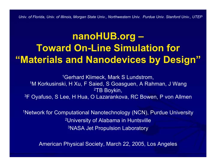

  1. Univ. of Florida, Univ. of Illinois, Morgan State Univ., Northwestern Univ. Purdue Univ. Stanford Univ., UTEP nanoHUB.org – Toward On-Line Simulation for “Materials and Nanodevices by Design” 1 Gerhard Klimeck, Mark S Lundstrom, 1 M Korkusinski, H Xu, F Saied, S Goasguen, A Rahman, J Wang 2 TB Boykin, 3 F Oyafuso, S Lee, H Hua, O Lazarankova, RC Bowen, P von Allmen 1 Network for Computational Nanotechnology (NCN), Purdue University 2 University of Alabama in Huntsville 3 NASA Jet Propulsion Laboratory American Physical Society, March 22, 2005, Los Angeles

  2. The NCN: Mission and Vision To support the National Nanotechnology Initiative through: • research • simulation tools • education and outreach • web-based services “To be the place where experiment, theory, and simulation meet and move nanoscience to nanotechnology.” NCN Morgan State University - Northwestern University - Purdue University - Stanford University - University of Florida - University of Illinois - University of Texas at El Paso 2

  3. Simulation is Essential for Nanotechnology Development Hint from the Semiconductor Industry: • No new devices / circuits designed without software! Simulation Problem: • Accepted nano simulation tool suite does NOT exist. Approach: • Conduct research in Modeling and Simulation of: • Nanoelectronics • Nanoelectromechanics • Nano-bio sensors • Computational science • DEVELOP and DEPLOY to nanoscience and nanotechnology community Fabrication Characterization NCN Morgan State University - Northwestern University - Purdue University - Stanford University - University of Florida - University of Illinois - University of Texas at El Paso 3

  4. NCN - Research nano-bio: nanoelectronics: NEMS: switches connecting molecules…. and sensors…. electronics and NEMS to biological systems V lipid 10.0 0.0 …to compact models protein water ….to MOSFETs -10.0 -30 -20 -10 0 10 20 30 Tip position (nm) 5.0 Tip Position (nm) S D 0.0 NCN 0.0 0.5 1.0 DC Bias (V) Morgan State University - Northwestern University - Purdue University - Stanford University - University of Florida - University of Illinois - University of Texas at El Paso 4

  5. electronics at the molecular scale Al Ultra-Scaled CMOS Gate HfO 2 D S 10 nm SiO 2 p ++ Si ~ 2 nm D G S ~ 5 nm SWNT ~1-4nm Molecules NCN Morgan State University - Northwestern University - Purdue University - Stanford University - University of Florida - University of Illinois - University of Texas at El Paso 5

  6. unifying view of small devices gate µ 1 µ 1 [ H ] [ � S ] S D [ � 2 ] [ � 1 ] non-equilibrium Green’s function approach (NEGF) NCN Morgan State University - Northwestern University - Purdue University - Stanford University - University of Florida - University of Illinois - University of Texas at El Paso 6

  7. The NCN: Mission and Vision To support the National Nanotechnology Initiative through: • research • simulation tools (1-D transport, 3-D, Synthesis) • education and outreach • web-based services “To be the place where experiment, theory, and simulation meet and move nanoscience to nanotechnology.” NCN Morgan State University - Northwestern University - Purdue University - Stanford University - University of Florida - University of Illinois - University of Texas at El Paso 7

  8. Resonant Tunneling Diode Current 12 different I-V curves: 2 wafers, 3 mesa sizes, 2 bias directions Voltage 50nm 1e18 InGaAs 7 ml nid InGaAs 7 ml nid AlAs Conduction band diagrams 20 ml nid InGaAs 7 ml nid AlAs for different voltages 7 ml nid InGaAs and the resulting current flow. 50 nm 1e18 InGaAs NCN Morgan State University - Northwestern University - Purdue University - Stanford University - University of Florida - University of Illinois - University of Texas at El Paso 8

  9. NEMO the first Nano CAD Tool originally developed at Texas Instruments Current Atomistic Basis Sets Concepts Voltage p x p p z s y 5x d 2x spin • • • • • • • • • • • Quantitative Design, Analysis, Synthesis NCN Morgan State University - Northwestern University - Purdue University - Stanford University - University of Florida - University of Illinois - University of Texas at El Paso 9

  10. NEMO Key Elements: Current Tight Binding sp 3 d 5 s* Realistically Extended Devices Concepts Non-Equilibrium Green Functions Voltage p x p p z s y 5x d 2x spin Transport / Engineering Quantum Mechanics / Quantitative Physics Design, Analysis, Synthesis NCN Morgan State University - Northwestern University - Purdue University - Stanford University - University of Florida - University of Illinois - University of Texas at El Paso 10

  11. Ultra Thin Body SOI: A traditional Quantum Well? Most basic Five Atomic Layer quantum mechanical problem: Si (001) Particle in a box! 2 nd IEDM, Uchida 2 nd Expect / Remember: 1 st 1 st • State quantization • 2 counter-propagating states • 1 bound state L k 1 = � quantize k Schrödinger Equation E L � E � h 2 d 2 � ( ) = e + ik 1 z 2 propagating ( ) ( ) = 0 dz 2 � V z � z ( ) = e � ik 1 z � z � � � z 2 m * states � � 1 bound ( ) = sin k 1 z ( ) � z E = h 2 k 2 Parabolic state Dispersion k 2 m * NCN Morgan State University - Northwestern University - Purdue University - Stanford University - University of Florida - University of Illinois - University of Texas at El Paso 11

  12. Quantum Wells - Special Considerations in Si Five Atomic layers Five Atomic Layer Si (001) 2 nd IEDM, Uchida TB ∆ E Sub 1 1 st Eff. mass Δ E=150meV= 6k B T effect at T=300K L k 1,2 = π /L k 1,2 = π /L 2 valleys 4 propagating states 2 bound states k 1,2 envelope k m fast oscillations NCN Morgan State University - Northwestern University - Purdue University - Stanford University - University of Florida - University of Illinois - University of Texas at El Paso 12

  13. The NCN: Mission and Vision To support the National Nanotechnology Initiative through: • research • simulation tools (1-D transport, 3-D , Synthesis) • education and outreach • web-based services “To be the place where experiment, theory, and simulation meet and move nanoscience to nanotechnology.” NCN Morgan State University - Northwestern University - Purdue University - Stanford University - University of Florida - University of Illinois - University of Texas at El Paso 13

  14. Quantum Dots: A Material / Device Testbed Multi-Million Atoms Simulations Designed Optical Transitions Sensors Quantum Dot Arrays Nanoscale Quantum States Atomic Orbitals Computing Structure (Artificial Atoms, size 20nm) size: 0.2nm Approach: Problem: •Use local orbital description for individual Nanoscale device simulation requirements: atoms in arbitrary crystal / bonding • Cannot use bulk / jellium descriptions, need configuration description of the material atom by atom •Use s, p, and d orbitals => use pseudo-potential or local orbitals Use GA for material parameter fitting • Consider finite extent/transport, not infinitely •Strain with VFF periodic •Custom eigensolver => local orbital approach • Demonstrated 64 Million Atom System • Need to include > 1 million atoms. Volume of => need massively parallel computers • 110x110x110 nm 3 • The design space is huge: choice of • 15x300x300 nm 3 materials, compositions, doping, size, shape. => need a design tool NCN Morgan State University - Northwestern University - Purdue University - Stanford University - University of Florida - University of Illinois - University of Texas at El Paso 14

  15. Alloy Disorder Results: Problem: • Simulated >1000 dots with random cation • Cations are randomly distributed in alloy distributions. dots. • Inhomogeneous broadening factor of • Does alloy disorder limit electronic ~0.5-5meV due to alloy disorder. structure uniformity for dot ensembles? Impact: Approach: • Fundamental uniformity limit for ensemble • Simulate a statistical ensemble of alloyed of alloy-based quantum dots. dots. • Requires atomistic simulation tool. Simulation of Alloy Dot Ensemble Γ =~0.5-5meV E eh =1.05eV In 0.6 Ga 0.4 As Lense Shaped Dot Diameter=30nm,Height=5nm, GaAs embedded ~1,000,000 Atom Simulation, sp3s * basis In and Ga atoms are randomly distributed Measured Γ =34.6 meV (R. Leon, PRB, 58 , R4262) Inhomegenious Broadening? Examined Theoretical Lower Limit NCN Morgan State University - Northwestern University - Purdue University - Stanford University - University of Florida - University of Illinois - University of Texas at El Paso 15

  16. Computational Nanotechnology NEMO 3-D: Electronic structure for 23 Million Atoms Performed on NSF Teragrid Result / Demonstrations / Impact: • 64 million atom strain - volume (110nm) 3 • 23 million atom electronic structure Volume (78nm) 3 or 15x178x178nm 3 • Determined long range extent of strain in self-assembled quantum dots NCN Morgan State University - Northwestern University - Purdue University - Stanford University - University of Florida - University of Illinois - University of Texas at El Paso 16

Download Presentation
Download Policy: The content available on the website is offered to you 'AS IS' for your personal information and use only. It cannot be commercialized, licensed, or distributed on other websites without prior consent from the author. To download a presentation, simply click this link. If you encounter any difficulties during the download process, it's possible that the publisher has removed the file from their server.

Recommend


More recommend