Relative Timing Driven Multi-Synchronous Design: Enabling - PowerPoint PPT Presentation
Relative Timing Driven Multi-Synchronous Design: Enabling Order-of-Magnitude Energy Reduction Kenneth S. Stevens University of Utah Granite Mountain Technologies 27 March 2013 UofU and GMT 1 Learn from Prof. Kajitana Think differently
Relative Timing Driven Multi-Synchronous Design: Enabling Order-of-Magnitude Energy Reduction Kenneth S. Stevens University of Utah Granite Mountain Technologies 27 March 2013 UofU and GMT 1
Learn from Prof. Kajitana ● Think differently and deeply ● Apply thought to current challenges Then collaborate Goals of Presentation: 1. Define and propose “rule breaker” idea 2. Request support from physical design community 27 March 2013 UofU and GMT 2
Multi-Synchronous Advantage 1. Efficiency in power and performance is new game in town 2. Multi-synchronous design provides optimization opportunity 3. New (asynchronous) timing model is one excellent path 4. Produces average 10 × e τ 2 improvement ● Pentium: e τ 2 = 17 . 5 × e τ 2 = 16 . 9 × ● FFT: 5. But ... need improved physical design support Design Energy Area Freq. Latency Aggregate 12.11 × Pentium F .E. 2.05 2.92 2.38 0.85 77.98 × 64-pt FFT 3.95 2.83 2.07 3.37 27 March 2013 UofU and GMT 3
Timing is a Key Issue Multi-synchronous design produces best results Synchronous Clock at 1.5GHz ✻ ✻ ✻ ✻ Async Synchronous ✛ ✲ ✛ ✲ circuit 3.0GHz clk ✻ ✻ Synchronous ✲ ✲ Pausable variable freq. 1.7GHz clk s ✲ s ✲ ❄ ❄ Synchronous Clock at 1.8GHz Single frequency, low skew Multiple frequencies (small blocks, standard CAD) (SoC reality – localization) 1. global block frequencies 1. blocks operate at best frequency 2. higher clock power 2. network not synchronized 3. clock design, distribution 3. synchronizing FIFOs 27 March 2013 UofU and GMT 4
Energy Efficient Design Wine goblet model: ● Energy efficiency has two primary sources ◆ System architecture ◆ Physical design arch ● Methodology and CAD unify sources Best realization: ● Multi-synchronous pd ◆ Defined by system’s critical path ◆ Then optimal local power-delay ◆ Asynchronous best methodology: ■ no synchronization cost 27 March 2013 UofU and GMT 5
Interface Matters! Clocked design requires synchronizers when crossing all domains. IP Clock Domain Network Clock Domain data clk s S S r S S Major location for buffering in a design. 27 March 2013 UofU and GMT 6
Interface Matters! No synchronization required into async domain. IP Clock Domain Network Clock Domain data clk s r S S Improves power, performance, and modularity 27 March 2013 UofU and GMT 7
Timed Asynchronous Designs 27 March 2013 UofU and GMT 8
Multi-Synchronous Architecture 1. Make architectural bottleneck as fast as possible. 2. Make the rest of the design match bottleneck ● . . . normally as slow as possible 3. Optimize locally for power/performance. L1 L7 irdy bufack tagout1 bufreq irdyack tagin1 tagout7 tagin7 Asynchronous Pentium bottleneck circuit 27 March 2013 UofU and GMT 9
Concurrency and Time Architectural level timing experiment: Pentium front end 5 Column 0 1 2 3 4 6 7 8 9 10 11 12 13 14 15 Cache Latch Len. Decoders Tag Units Row 0 Output Buffer Tag Units Row 1 Output Buffer Row 2 Tag Units Output Buffer Tag Units Row 3 Output Buffer 27 March 2013 UofU and GMT 10
Concurrency and Time Architectural level timing experiment: Pentium front end Target Cache Latch Len. Decoders 3 3 9 4 1 7 2 1 6 3 5 3 5 1 3 4 1 Tag Units Output Buffer 2 Tag Units Output Buffer Tag Units Output Buffer Tag Units Output Buffer 27 March 2013 UofU and GMT 11
Concurrency and Time Architectural level timing experiment: Pentium front end Cache Latch Len. Decoders 3 1 7 2 1 6 3 5 3 5 1 3 4 1 Tag Units Output Buffer 2 Tag Units Output Buffer 3 Tag Units Output Buffer Tag Units Output Buffer 27 March 2013 UofU and GMT 12
Concurrency and Time Architectural level timing experiment: Pentium front end Cache Latch Len. Decoders 3 2 1 4 7 2 1 6 3 5 3 5 1 3 4 1 Tag Units Output Buffer 2 Tag Units Output Buffer 3 Tag Units Output Buffer 4 Tag Units Output Buffer 27 March 2013 UofU and GMT 13
Concurrency and Time Architectural level timing experiment: Pentium front end Cache Latch Len. Decoders 3 2 1 4 2 5 1 3 4 5 Tag Units Output Buffer 2 Tag Units Output Buffer 3 Tag Units Output Buffer 4 Tag Units Output Buffer 27 March 2013 UofU and GMT 14
Concurrency and Time Architectural level timing experiment: Pentium front end Cache Latch Len. Decoders 2 1 4 2 3 1 7 9 4 2 3 5 Tag Units Output Buffer 6 2 Tag Units Output Buffer 3 Tag Units Output Buffer 4 Tag Units Output Buffer 27 March 2013 UofU and GMT 15
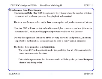
Timing and Sequencing Traditional representation of timing: ● Metric values ◆ On an IC we measure it to picoseconds ◆ In track and ski racing, we measure it to milliseconds But what do we really care about? ● it isn’t the number on the stop watch. . . 27 March 2013 UofU and GMT 16
Timing and Sequencing Traditional representation of timing: ● Metric values ◆ On an IC we measure it to picoseconds ◆ In track and ski racing, we measure it to milliseconds But what do we really care about? ● it isn’t the number on the stop watch. . . We care about who wins!! The key: Timing results in sequencing Relative Timing formally represents the signal sequencing produced by circuit timing 27 March 2013 UofU and GMT 17
New Formal Abstract Model: Relative Timing ● Timing is both the technology differentiator and barrier ● Relative Timing is the generalized solution ● The key property of time is the sequencing it imposes Sequence gives winner, performance, etc. ● true in semiconductors as well as sports ● absolute stopwatch value is auxiliary Novel relativistic formal logic representation of time (relative timing): pod �→ poc 1 ≺ poc 2 Sequencing relative to common reference ● can now evaluate sequencing ● can now control sequencing 27 March 2013 UofU and GMT 18
Relative Timing 1. Relative Timing ● Sequences signals at poc ( point of convergence ) ● Requires a common timing reference: pod ( point of divergence ) 2. Formal representation: pod �→ poc 1 + margin ≺ poc 2 3. RT models timing in ALL systems pod = clock poc = flops ● Clocked: pod = request poc = latches ● Async: 4. RT enables direct commercial CAD support of general timing requirements ● formal RT constraints mapped to sdc constraints data FF i FF i+1 POC 0 clk A POD POC POD POC 1 clk B i i+1 data m 27 March 2013 UofU and GMT 19
Relative Timed Design: Bundled Data Bundled data design is much like clocked. n n n n C C C C L i + 1 L i + 2 FF i + FF i + L i FF i L L L L 1 2 clock network req i req i + 1 req i + 2 req i + 3 delay delay Ctl i Ctl i + 1 Ctl i + 2 ack i + 1 ack i + 2 ack i + 3 ack i Frequency based (clocked) design. Timed (bundled data) handshake Clock frequency and datapath delay of design. Delay element sized by first pipeline stage is constrained by RT constraint: L i /clk ↑ i �→ L i + 1 /d+s ≺ L i + 1 /clk ↑ i + 1 req i ↑ �→ L i + 1 /d+s ≺ L i + 1 /clk ↑ Clocked physical design directly supports the clocked Relative Timing constraints. The asynchronous circuit constraints must be provided as min and max constraints, and are not well supported 27 March 2013 UofU and GMT 20
Relative Timing Driven Flow set d0 fdel 0.600 set d0 fdel margin [expr $d0 fdel + 0.050] set d0 bdel 0.060 set size only -all instances [find -hier cell lc1] set size only -all instances [find -hier cell lc3] set size only -all instances [find -hier cell lc4] set disable timing -from A2 -to Y [find -hier cell lc1] set disable timing -from B1 -to Y [find -hier cell lc1] set disable timing -from A2 -to Y [find -hier cell lc3] set disable timing -from B1 -to Y [find -hier cell lc3] set max delay $d0 fdel -from a -to l0/d set max delay $d0 fdel -from b -to l0/d set min delay $d0 fdel margin -from lr -to l0/clk set max delay $d0 bdel -from lr -to la #margin 0.050 -from a -to l0/d -from lr -to l0/clk #margin 0.050 -from b -to l0/d -from lr -to l0/clk 27 March 2013 UofU and GMT 21
Multi-rate 64-Point FFT Architecture Initial design target: high performance military applications ● Mathematically based on W N = e − j 2 π N notation ● Hierarchical multi-rate design: N = N 1 N 2 ● Decimate frequency ( ↓ ) by N 2 ◆ operate on N 2 low frequency streams ● Transmute data & frequency to N 1 low frequency streams ● Expand ( ↑ ) by N 1 to reconstruct original frequency stream 27 March 2013 UofU and GMT 22
Design Models Hierarchical derivation of multi-frequency design: � � N 2 − 1 N 1 − 1 W m 1 n 2 n 1 = 0 x n 2 ( n 1 ) W m 1 n 1 W m 2 n 2 X m 1 ( m 2 ) = ∑ ∑ n 2 = 0 N N 1 N 2 ● N 2 FFTs using N 1 values as the inner summation ● Scaled and used to produce N 1 FFTs of N 2 values Hierarchically scale design ● Base case when N = 4 , X ( m ) = W 4 x ( n ) ● 4-point FFT performed without multiplication ◆ Multiplication constants W 4 become ± 1 27 March 2013 UofU and GMT 23
FFT-64 Implemented on IBM’s 65nm 10sf process, Artisan academic library Three design blocks: ● FFT-4 N 1 , N 2 = 4 ● FFT-16 N 1 = 16 , N 2 = 4 ● FFT-64 Two designs: ● Clocked Multi-Synchronous ● Relative Timed Multi-Synchronous ◆ near identical architectures ◆ additional RT area / pipeline optimized version for FFT-64 27 March 2013 UofU and GMT 24
Recommend
More recommend
Explore More Topics
Stay informed with curated content and fresh updates.

