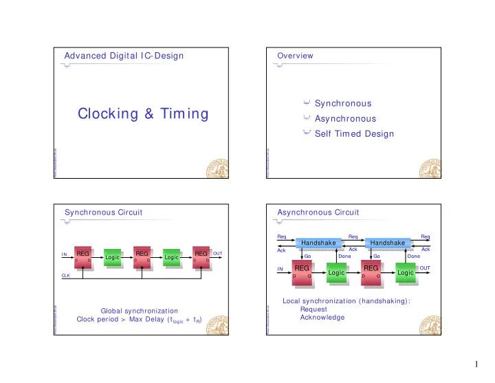
SLIDE 9 9
Skew Analysis - Example
R1
M U X
L L L R2 R3 L L L lk
- a. Determine the minimum clock period time if clock skew is disregarded.
- b. Determine the minimum clock period time if there is 1ns positive clock skew between
adjacent registers.
- c. Determine the minimum clock period time if there is 3ns positive clock skew between
adjacent registers.
- d. Calculate the maximum “clock skew” for the datapath, both positive and negative if the
clk Positive "clock skew"
- d. Calculate the maximum clock skew for the datapath, both positive and negative if the
clock signal has a period of 16ns. Register R setup time t S 0.5 ns Register R delay time t R 0.5 ns Logic L delay time t L 3.0 ns Mux delay time t M 1.0 ns
R1
M U X
L L L R2 R3 L L L lk
minimum clock period time if clock
Skew Analysis - Example
Answer: The minimum clock period time is 10 ns clk Positive "clock skew" skew is disregarded R2 to R3, t R+ 3t L+ t S = 0.5+ 3* 3.0+ 0.5 = 10ns R2 to R2, t R+ 2t L+ t m+ t S = 0.5+ 2* 3.0+ 1.0+ 0.5 = 8ns R1 to R2, t R+ 2t L+ t m+ t S = 0.5+ 2* 3.0+ 1.0+ 0.5 = 8ns Answer: The minimum clock period time is 10 ns
Register R setup time t S 0.5 ns Register R delay time t R 0.5 ns Logic L delay time t L 3.0 ns Mux delay time t M 1.0 ns
R1
M U X
L L L R2 R3 L L L lk
minimum clock period time if there is 1ns positive clock skew
Skew Analysis - Example
R2 to R3, t R+ 3t L+ t S-t SKEW = 0.5+ 3* 3.0+ 0.5-1 = 9ns Answer: The minimum clock period time is 9 ns clk Positive "clock skew" between adjacent registers.
Register R setup time t S 0.5 ns Register R delay time t R 0.5 ns Logic L delay time t L 3.0 ns Mux delay time t M 1.0 ns
R1
M U X
L L L R2 R3 L L L lk
minimum clock period time if there is 3ns positive clock skew
Skew Analysis - Example
R2 to R2, t R+ 2t L+ t m+ t S = 0.5+ 2* 3.0+ 1.0+ 0.5 = 8ns (No skew in feedback) clk Positive "clock skew" between adjacent registers
Register R setup time t S 0.5 ns Register R delay time t R 0.5 ns Logic L delay time t L 3.0 ns Mux delay time t M 1.0 ns