
SLIDE 1
Digital Design Discussion: RTL Storage Components Shift Register - - PowerPoint PPT Presentation
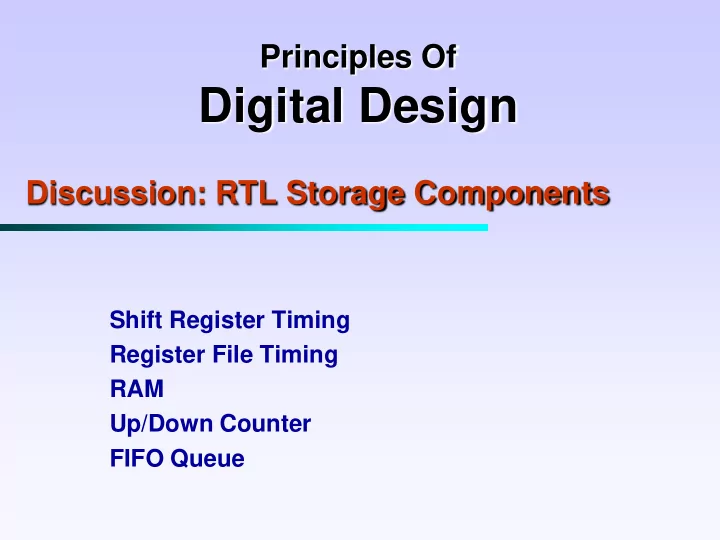
Principles Of Digital Design Discussion: RTL Storage Components Shift Register Timing Register File Timing RAM Up/Down Counter FIFO Queue Shift Register Timing Problem: Complete the timing diagram for the shift register shown. Assume
RTL Storage Components DIGITAL DESIGN 101, University of California
Problem: Complete the timing diagram for the shift
Present State Operation S1 S0
No Shift 1 Load Input 1 Shift Left 1 1 Shift Right
Q0 D0 3 Selector Selector Selector Selector Q1 D1 Q2 D2 Q3 D3 1 2 3 1 2 3 1 2 3 1 2
I3 I2 I1 I0 Y3 Y2 Y1 Y0 IL IR S1 S0 Clk Shifter Timing Diagram Shifter Schematic Shifter Truth Table
2
I3 I2 I1 I0 Clk Q3 Q2 Q1 Q0 S1 S0 t0 t1 t2 t3 t4
RTL Storage Components DIGITAL DESIGN 101, University of California
Solution: Complete the timing diagram…
I3 I2 I1 I0 Clk Q3 Q2 Q1 Q0 S1 S0 t0 t1 t2 t3 t4
Present State Operation S1 S0
No Shift 1 Load Input 1 Shift Left 1 1 Shift Right
Q0 D0 3 Selector Selector Selector Selector Q1 D1 Q2 D2 Q3 D3 1 2 3 1 2 3 1 2 3 1 2
I3 I2 I1 I0 Y3 Y2 Y1 Y0 IL IR S1 S0 Clk Shifter Timing Diagram Shifter Schematic Shifter Truth Table
3
RTL Storage Components DIGITAL DESIGN 101, University of California
Problem: Complete the timing diagram for the register
4
RF Timing Diagram RF Schematic
RFC RFC RFC RFC RFC RFC RFC RFC RFC RFC RFC RFC RFC RFC RFC RFC 1 2 3 1 2 3 1 2 3 2-to-4 Write Decoder 2-to-4 Read Decoder 2-to-4 Read Decoder
I3 I2 I1 I0 B3A3 B2A2 B1A1 B0A0 WA1 WA0 WE RAB1 RAB0 REB RAA1 RAA0 REA I3 I2 I1 I0 Clk A3 A2 A1 A0 WA WE RA
3 1 3
t0 t1 t2 t3 t4
RTL Storage Components DIGITAL DESIGN 101, University of California
Solution: Complete the timing diagram…
5
RF Timing Diagram RF Schematic
RFC RFC RFC RFC RFC RFC RFC RFC RFC RFC RFC RFC RFC RFC RFC RFC 1 2 3 1 2 3 1 2 3 2-to-4 Write Decoder 2-to-4 Read Decoder 2-to-4 Read Decoder
I3 I2 I1 I0 B3A3 B2A2 B1A1 B0A0 WA1 WA0 WE RAB1 RAB0 REB RAA1 RAA0 REA I3 I2 I1 I0 Clk A3 A2 A1 A0 WA WE RA
3 1 3
t0 t1 t2 t3 t4
RTL Storage Components DIGITAL DESIGN 101, University of California
Timing diagram
Reading address 1 Writing 1110 to address 3 Reading address 3 Writing 0110 to address 3
I3 I2 I1 I0 Clk A3 A2 A1 A0 WA WE RA
3 1 3
6
RTL Storage Components DIGITAL DESIGN 101, University of California
Build 1M x 32 RAM using 256 K x 32 RAM chips.
. . . . . . . . .
CS I31 I1 I0 A17 A1 A0 RWS
218 x 32 RAM
. . . . . . O31 O1 O0 . . . . . . . . . . . . Memory address and content
7
RTL Storage Components DIGITAL DESIGN 101, University of California
8
RWS Input bus Output bus
I A CS RWS O M0
Addresses 218-1
. . .
219-1
. . .
218 219+218-1
. . .
219 220-1
. . .
219+218
Four 256K RAM 256 K = 28 X 210 = 218
1 M = 220
the four 256 K x 32 RAM chips via decoder
I A CS RWS O M1 I A CS RWS O M2 I A CS RWS O M3 18 1 2 3 2-to-4 decoder 2
8
RTL Storage Components DIGITAL DESIGN 101, University of California
Design a circuit that outputs a 1 every 60 clock cycles using
Q0 Q1 Q2 Q3
Up/Down Counter E Reset D
Q4 Q5 Q6 Q7
E D Operations
0 X 1 0 1 1 No change Count up Count down
60 is 00111100 Reset count when it reaches 60 by setting Reset = 0
Q0 Q1 Q2 Q3
Up/Down Counter E Reset D
Q4 Q5 Q6 Q7
9
1 Clk OUT
0 0 1 1 1 1 0 0
RTL Storage Components DIGITAL DESIGN 101, University of California
Complete timing diagram for a FIFO queue. Assume all
Clk READ/WRITE IN
42 100 8
OUT
10
RTL Storage Components DIGITAL DESIGN 101, University of California
11
23 Back Front 34 empty empty 45 34 23 empty 23
45
45 34 empty empty
empty data empty data Front Back 1 2 1021 1022 1023
. . .
empty data
Front E Reset Back E Reset Selector 1 S A CS RWS 1K RAM Comparator < = > 10 10 1 1
Reset Read/ write Enable I/O b Emp Full Clk
No change Read Write X 0 0 1 1 1
Operations Read/Write Enable
No change Read Write X 0 0 1 1 1
Operations Read/Write Enable
RTL Storage Components DIGITAL DESIGN 101, University of California
12
Front E Reset Back E Reset Selector 1 S A CS RWS 1K RAM Comparator < = > 10 10 1 1
Reset Read/ write Enable I/O bus Empty Full Clk
t 42
Clk READ/ WRITE IN OUT
42 100 8 t
100
8
First in , first out Counters update at clk’s positive edge
12
No change Read Write X 0 0 1 1 1
Operations Read/Write Enable
No change Read Write X 0 0 1 1 1
Operations Read/Write Enable