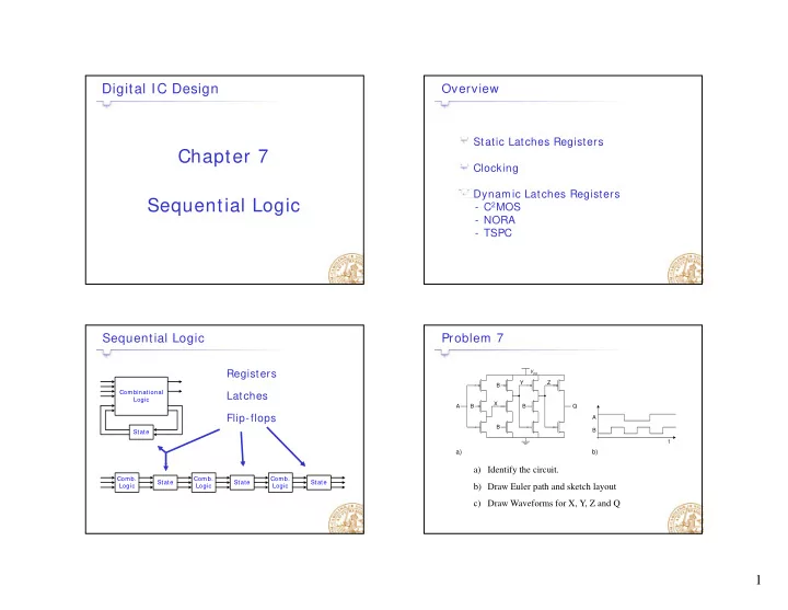
chapter 7
play

Chapter 7 Clocking Dynamic Latches Registers Sequential Logic q - PowerPoint PPT Presentation

Digital IC Design Overview Static Latches Registers Static Latches Registers Chapter 7 Clocking Dynamic Latches Registers Sequential Logic q g - C 2 MOS - NORA - TSPC Sequential Logic Problem 7 Registers V DD Y Z B Combinational


  1. Digital IC Design Overview Static Latches Registers Static Latches Registers Chapter 7 Clocking Dynamic Latches Registers Sequential Logic q g - C 2 MOS - NORA - TSPC Sequential Logic Problem 7 Registers V DD Y Z B Combinational Latches Latches Logic X A B B Q Flip-flops A B B State t a) b) a) Identify the circuit. Comb. Comb. Comb. State State State Logic Logic Logic b) Draw Euler path and sketch layout c) Draw Waveforms for X, Y, Z and Q 1

  2. Problem 7 - Solution Digital IC Design V DD Y Z B b) Y X X Chapter 11 h A B B Q Q B Arithmetic A B Z X Building Blocks g A c) c) B B X Y Z Q t Binary Adder Binary Adder Cell (Two’s Complement) Half Adder A B A B B C i S C o A = ⊕ S A B HA C o HA C o 0 0 0 0 0 0 0 0 0 Delete 0 Delete = C AB 0 0 1 1 0 Delete S S o 0 1 0 1 0 Propagate A B A B 0 1 1 0 1 Propagate Full adder C i FA C o C i FA C o 1 0 0 1 0 Propagate = ⊕ ⊕ = S A B C S S 1 1 0 0 1 1 0 0 1 Propagate 1 Propagate A B A B = + + + ABC ABC ABC ABC 1 1 0 0 1 Generate C i C o C i C o = + + 1 1 1 1 1 Generate C AB AC BC o S S 2

  3. Problem 4 Problem 4 - Solution Bit # 5 4 3 2 1 0 = Delete, A 1 0 1 0 1 1 D A B P i P i+1 B 1 0 0 1 0 1 a) What is the name and purpose = ⊕ Propagate, P A B Generate 1 0 0 0 0 1 P i P G G i P P i+1 G i+1 G of this unit? f hi i ? = Generate, G AB Propagate 0 0 1 1 1 0 Delete 0 1 0 0 0 0 b) Draw the architecture of a 6-bit P 0 P 1 P 2 P 3 P 4 P 5 C in C i+1 adder using this unit. Carry Carry P 0 G 0 P 1 G 1 P 2 G 2 P 3 G 3 P 4 G 4 P 5 G 5 c) Show longest path if C in Carry Carry Carry Carry Carry Carry Sum Sum A = 101011 and B = 100101 Sum Sum Sum Sum Sum Sum Sum Sum Sum Sum Sum Sum S i S i+1 d) Suggest simplification to first S 0 S 1 S 2 S 3 S 4 S 5 and last module. What I believe to be longest path! Solution manual Digital IC Design Problem 6 WL WWL V dd WL RWL M4 M2 M Q Q 3 Q M6 M M M5 1 2 M Chapter 12 1 C M1 M3 S C S BL BL1 BL2 BL BL Memories a) Describe the functional difference between the three RAM cells. b) Describe a write-read cycle for each. 3

  4. 6-transistor SRAM Cell 3 transistor DRAM Cell Write cycle WL V DD WWL BL1 V dd V dd M4 M2 WWL Flip-Flop RWL R Q Q introduced in M 3 M6 X M5 W Chapter 7 X V DD -V T M 1 M 2 M1 M3 Read cycle C S RWL Transistor sizing Transistor sizing BL BL BL BL important to ensure Δ V BL2 V DD -V T BL1 BL2 functionality Write Read Inversed Value is Read Restore of 1 transistor DRAM Cell V BL V(1) BL WL WL Δ V(1) = small change V Pre M 1 C S V(0) C BL Sense amp. activated Word line activated Destructive Read, needs restore! Feedback of sense amplifier output to BL 4

Download Presentation
Download Policy: The content available on the website is offered to you 'AS IS' for your personal information and use only. It cannot be commercialized, licensed, or distributed on other websites without prior consent from the author. To download a presentation, simply click this link. If you encounter any difficulties during the download process, it's possible that the publisher has removed the file from their server.

Recommend


More recommend