PCB Technical Capacity (2012.10 Updated) No. Item Capacity for - - PowerPoint PPT Presentation

pcb technical capacity 2012 10 updated
SMART_READER_LITE
LIVE PREVIEW

PCB Technical Capacity (2012.10 Updated) No. Item Capacity for - - PowerPoint PPT Presentation

Page 1 of 7 PCB Technical Capacity (2012.10 Updated) No. Item Capacity for sample Capacity for small & medium production 1 FR4(General) Brand: Shengyi, Guoji, KB, ITEQ Brand: Shengyi, Guoji, KB, ITEQ 2 Halogen Free S1155(General TG),


slide-1
SLIDE 1

Page 1 of 7

PCB Technical Capacity (2012.10 Updated)

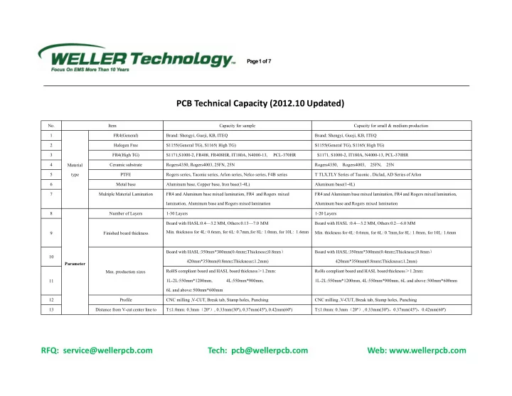
No. Item Capacity for sample Capacity for small & medium production 1 Material type FR4(General) Brand: Shengyi, Guoji, KB, ITEQ Brand: Shengyi, Guoji, KB, ITEQ 2 Halogen Free S1155(General TG), S1165( High TG) S1155(General TG), S1165( High TG) 3 FR4(High TG) S1171,S1000-2, FR408, FR408HR, IT180A, N4000-13, PCL-370HR S1171, S1000-2, IT180A, N4000-13, PCL-370HR 4 Ceramic substrate Rogers4350, Rogers4003, 25FN, 25N Rogers4350, Rogers4003, 25FN, 25N 5 PTFE Rogers series, Taconic series, Arlon series, Nelco series, F4B series T TLX,TLY Series of Taconic , Diclad, AD Series of Arlon 6 Metal base Aluminum base, Copper base, Iron base(1-4L) Aluminum base(1-4L) 7 Mulriple Material Lamination FR4 and Aluminum base mixed lamination, FR4 and Rogers mixed lamination, Aluminum base and Rogers mixed lamination FR4 and Aluminum base mixed lamination, FR4 and Rogers mixed lamination, Aluminum base and Rogers mixed lamination 8 Parameter Number of Layers 1-30 Layers 1-20 Layers 9 Finished board thickness Board with HASL:0.4—3.2 MM, Others:0.13—7.0 MM

  • Min. thickness for 4L: 0.6mm, for 6L: 0.7mm,for 8L: 1.0mm, for 10L: 1.6mm

Board with HASL :0.4—3.2 MM, Others:0.2—6.0 MM

  • Min. thickness for 4L: 0.6mm, for 6L: 0.7mm,for 8L: 1.0mm, for 10L: 1.6mm

10

  • Max. production sizes

Board with HASL:350mm*300mm(0.4mm≤Thickness≤0.8mm) 420mm*350mm(0.8mm≤Thickness≤1.2mm) Board with HASL:350mm*300mm(0.4mm≤Thickness≤0.8mm) 420mm*350mm(0.8mm≤Thickness≤1.2mm) 11 RoHS compliant board and HASL board thickness>1.2mm: 1L-2L:550mm*1200mm, 4L:550mm*900mm, 6L and above: 500mm*600mm RoHs compliant board and HASL board thickness>1.2mm: 1L-2L:550mm*1200mm, 4L:550mm*900mm, 6L and above: 500mm*600mm 12 Profile CNC milling ,V-CUT, Break tab, Stamp holes, Punching CNC milling ,V-CUT, Break tab, Stamp holes, Punching 13 Distance from V-cut center line to T≤1.0mm: 0.3mm(20º), 0.33mm(30º), 0.37mm(45º), 0.42mm(60º) T≤1.0mm: 0.3mm(20º), 0.33mm(30º),0.37mm(45º),0.42mm(60º)

RFQ: service@wellerpcb.com Tech: pcb@wellerpcb.com Web: www.wellerpcb.com

slide-2
SLIDE 2

Page 2 of 7

14 circuits of Inner & outer layer 1.0mm<T≤1.6mm: 0.36mm(20º),0.4mm(30º),0.5mm(45º),0.6mm(60 º) 1.0mm<T≤1.6mm:0.36mm(20º),0.4mm(30º),0.5mm(45º),0.6mm(60º) 15 1.6mm<T≤2.4mm::0.42mm(20º),0.5mm(30º),0.6mm(45º),0.8mm(60º) 1.6mm<T≤2.4mm:0.42mm(20º),0.5mm(30º),0.6mm(45º),0.8mm(60º) 16 2.4mm<T≤3.0mm: 0.47mm(20º),0.6mm(30º),0.8mm(45º),1.0mm(60º) 2.4mm<T≤3.0mm: 0.47mm(20º),0.6mm(30º),0.8mm(45º),1.0mm(60º) 17 Drilling Hole Mechanical hole(Finished) 0.1mm≤Hole Dia.≤6.2mm (Driller size:0.15mm—6.3mm) 0.15mm≤Hole Dia.≤6.2mm (Drilling size:0.2mm—6.3mm) 18

  • Min. finished hole for PTFE and Mulriple Material Lamination:0.35MM

(Driller size:0.45mm)

  • Min. finished hole for PTFE and Mulriple Material Lamination:0.35MM (Driller

size:0.45mm) 19 Mechanical blind/buried hole Dia.≤0.3mm (Driller size≤0.4mm) Mechanical blind/buried hole Dia.≤0.3mm (Driller size≤0.4mm) 20 Drilling Hole Mechanical hole(Finished)

  • Min. Width for Slot: 0.5mm (Min. Router size :0.6mm)
  • Min. Width for Slot: 0.5mm (Min. Router size :0.6mm)

21

  • Min. Jointed hole Dia.: 0.35mm (Driller size:0.45mm)
  • Min. Jointed hole Dia.: 0.35mm (Driller size:0.45mm)

22

  • Dia. For Hole plugged with solder mask≤0.3mm (Driller size≤0.4mm)
  • Dia. For Hole plugged with solder mask≤0.3mm (Driller size≤0.4mm)

23 0.1mm≤Finished Dia. for hole plugged with resin≤0.4mm 0.1mm≤Finished Dia. for hole plugged with resin≤0.4mm 24 Laser drilling hole(Finished) Minimum Finished laser drilling hole Diameter: 0.1mm(Depth≤65um) 0.13mm(Depth≤100um) / 25 0.075mm≤Finished Dia. For blind hole plugged with resin≤0.15mm / 26 0.075mm≤Finished Dia. For blind hole plugged with plated copper≤0.127mm / 27 Back drilling hole 0.5mm≤Back drilling hole Dia.≤6.5mm 0.5mm≤Back drilling hole Dia.≤6.5mm 28 Countersink hole, Step hole Standard drilling:130° (Driller Dia.≤3.175mm),165° (3.175mm≤Driller Dia.≤6.3mm) Special drilling:82°,90°,120°(0.3mm≤Countersink hole drilling Dia.≤10mm) Standard drilling:130° ( Driller Dia.≤3.175mm ) ,165° ( 3.175mm≤Driller Dia.≤6.3mm) Special drilling:82°,90°,120°(0.3mm≤Countersink hole drilling Dia.≤10mm) 29 30 Min hole & Aspect Ratio 0.1mm (T≤0.6mm) 0.15mm (T≤1.2mm)

  • Max. Aspect Ratio: 16:1(Min. drilling>0.2mm)

0.1mm (T≤0.6mm) 0.15mm (T≤1.2mm)

  • Max. Aspect Ratio: 16:1(Min. drilling>0.2mm)

31 32 Circuit graphic Copper weight Inner layer: 1/3 OZ – 4 OZ, Out layer: 1/2 OZ – 4 OZ 2L: Max. 6oz Inner lay: 1/3 OZ – 3 OZ, Outer layer: 1/2 OZ – 3 OZ 2L: Max. 6oz 33 Capacity for Inner layer Etching 1/3 OZ,1/2 OZ 3 / 3 mil 1/3 OZ,1/2 OZ 3 / 3 mil 34 1 OZ 3 / 4 mil 1 OZ 3 / 4 mil

RFQ: service@wellerpcb.com Tech: pcb@wellerpcb.com Web: www.wellerpcb.com

slide-3
SLIDE 3

Page 3 of 7

35 2 OZ 4 / 5 mil 2 OZ 4 / 5 mil 36 3 OZ 6 / 7 mil 3 OZ 7 / 9 mil 37 4 OZ 8 / 11 mil 4 OZ 9 / 12 mil 38 Capacity for Outer layer Etching 1/3 OZ 3 / 3 mil 1/3 OZ 3.5 / 4.5 mil 39 1/2 OZ 3 / 4 mil 1/2 OZ 4 / 4.5 mil 40 1 OZ 4.5 / 5 mil 1 OZ 5 / 5.5 mil 41 2 OZ 6 / 8 mil 2 OZ 6.5 / 8 mil 42 3 OZ 8/ 12 mil 3 OZ 8/ 13 mil 43 4 OZ 9/ 15 mil 4 OZ 10/ 16 mil 44 5 OZ 11/ 16 mil 5 OZ 12/ 18 mil 45 Circuit graphic Capacity for Outer layer Etching 6 OZ 13/ 18 mil 6 OZ 14/ 20 mil 46

  • Min. Distance from drilling hole to

copper(for blind hole) 8 mil (First stack up),9 mil (Second stack up ),10 mil (Third Stack up) 9 mil (First Stack up),10 mil (Second stack up) 47

  • Min. Distance from drilling hole to

copper(without blind hole) 6 mil(<8L), 7 mil (8L≤Layer≤12L), 8 mil (L>12L) 7 mil (<8L), 8 mil (8L≤L≤12L) 48

  • Min. Distance from laser drilling

hole to copper(HDI board) 6 mil 7 mil 49

  • Min. distance from Outline to

Inner/Outer circuit graphic 8 mil 8 mil 50

  • Min. space for inner layer isolated

area 8 mil 8 mil 51

  • Min. space for inner layer copper

from board edge to avoid exposure. 8 mil 8 mil 52

  • Min. Distance from gold finger

8 mil 10 mil

RFQ: service@wellerpcb.com Tech: pcb@wellerpcb.com Web: www.wellerpcb.com

slide-4
SLIDE 4

Page 4 of 7

Chamfer to circuit graphic 53

  • Min. space between wall of hole on

different network 8 mil 10 mil 54

  • Min. Distance between pads with

Immersion gold 4 mil 5 mil 55

  • Min. Distance between pads with

HASL( No solder mask) 6 mil (Isolation 10mil for pads on copper) 7 mil (Isolation 10mil for pads on copper) 56

  • Min. Annular ring for Vias

14 mil (8 mil Hole Dia. , H/1 OZ base copper), 20 mil (8 mil Hole Dia. , 2 OZ base copper) 18 mil (8 mil Hole Dia., H/1 OZ base copper), 24 mil (8 mil Hole Dia., 2 OZ base copper) 57

  • Min. Annular ring for DIP holes

20 mil (8 mil Hole Dia., H/1 OZ base copper ), 24 mil (8 mil Hole Dia.,2 OZ base copper) 22 mil (8 mil Hole Dia., H/1 OZ base copper), 26 mil (8 mil Hole Dia.,2 OZ base copper) 58

  • Min. pads for BGA(Finished)

Immersion gold, Immersion silver, Immersion Tin, OSP≥7 mil HASL: Isolated circuit ≥8 mil, Solder mask opening on copper≥14 mil Immersion gold, Immersion silver, Immersion Tin, OSP:≥10 mil HAL: Isolated circuit≥10 mil, Solder mask opening on copper≥16 mil 59 60

  • Min. width/ space for grid

7/7 mil 7/7 mil 61

  • Min. space between gold fingers

6 mil 7 mil 62 Colors for solder mask inks Green, Yellow, Red, White, Blue, Black, Matt Black, Matt Green Green, Yellow, Red, White, Blue, Black, Matt Black, Matt Green 63 Silkscreen Colors for Silkscreen White, Yellow, Black, Grey, Orange White, Yellow, Black, Grey, Orange 64

  • Min. Width for solder mask bridge

Base copper≤1 OZ,4 mil(Green),5mil (Other colors) Base copper:2-4 OZ, 6mil. Base copper≤1 OZ,4 mil(Green),5mil (Other colors) Base copper: 2-4 OZ, 6mil. 65 66

  • Min. single width for solder mask
  • pening

2 mil (Partial 1.5 mil) 2.5 mil (Partial 2 mil) 67

  • Min. Width & Height for silkscreen
  • Min. Width:5 mil, Min. height: 28 mil
  • Min. Width:5 mil, Min. height: 28 mil

68 Type for silkscreen(only for white color) Serial number, Bar code, Two-dimension code Serial number, Bar code, Two-dimension code

RFQ: service@wellerpcb.com Tech: pcb@wellerpcb.com Web: www.wellerpcb.com

slide-5
SLIDE 5

Page 5 of 7

69

  • Min. space from peel able solder

mask to pad 14 mil 16 mil 70

  • Min. space from silkscreen to pad 6 mil

8 mil 71

  • Min. space from Carbon to pad

10 mil 12 mil 72

  • Min. space from carbon to carbon 13 mil

16 mil 73 Surface finishing RoHs compliant HASL(Lead free),Immersion gold, Immersion Tin, Immersion Silver, OSP, Hard Gold, Immersion gold + OSP, Immersion gold + Plated gold fingers, Gold plated + Plated gold fingers, Immersion Silver + Plated gold fingers, Immersion Tin + Plated gold fingers, ENEPIG, Pattern plated(Base copper≤2 OZ) HASL(Lead free),Immersion gold, Immersion Tin, Immersion Silver, OSP, Immersion gold + Plated gold fingers, Gold plated + Plated gold fingers, Immersion Silver + Plated gold fingers, Immersion Tin + Plated gold fingers, ENEPIG , Pattern plated(Base copper ≤2 OZ) 74 75 76 No RoHs compliant HASL HASL 77 Surface plating and Coating thickness HASL 2-40 um (0.4um Large Tin area) 2-40 um (0.4um Large Tin area) 78 Pattern plated Nickel:3um-5um, Gold :0.025um-0.1 um Nickel:3um-5um, Gold :0.025um-0.1 um 79 Immersion gold Nickel:3um-5um, Gold :0.05um-0.1 um Nickel:3um-5um, Gold :0.05um-0.1 um 80 Immersion Tin ≥1.0 um ≥1.0 um 81 Immersion silver 0.1 um-0.3 um 0.1 um-0.3 um 82 OSP 0.2 um-0.3 um 0.2 um-0.3 um 83 Plated hard gold ≤3 um (2.0 um or more need to review) ≤3 um (0.8 um or more need to review) 84 Chemical Nickel& Pd Gold Soldering: Nickel:3 um-5 um, Pd: 05 um-0.1 um, Gold: 0.03 um-0.05 um Bonding: Nickel:3 um-5 um, Pd: 0.1 um-0.15 um, Gold: 0.07 um-0.15 um Soldering: Nickel:3 um-5 um, Pd: 0.05 um-0.1 um, Gold:0.03 um-0.05 um Bonding: Nickel:3 um-5 um, Pd: 0.1 um-0.15 um, Gold: 0.07 um-0.15 um 85 86 Solder mask 15 um-25 um( solder mask on copper), 8 um-12 um( solder mask on via and the edge of circuit) (Once) 15 um-25 um(solder mask on copper),8 um-12 um(solder mask on via and the edge

  • f circuit) (Once)

87 KEY CARBONIZED 0.1 um-0.35 um 0.1 um-0.35 um 88 Peelable mask 0.2 um-0.5 um 0.2 um-0.5 um

RFQ: service@wellerpcb.com Tech: pcb@wellerpcb.com Web: www.wellerpcb.com

slide-6
SLIDE 6

Page 6 of 7

89 Tolerance PTH + / - 0.076 um + / - 0.076 um 90 NPTH + / - 0.05 um + / - 0.05 um 91 Press-fit + / - 0.05 um + / - 0.05 um 92 Precision of hole location + / - 0.076 um + / - 0.076 um 93 Angle of counter-boring + / - 10º + / - 10º 94 Orifice of counter-boring + / - 0.2 mm + / - 0.2 mm 95 Depth of counter-boring + / - 0.2 mm + / - 0.2 mm 96 Precision of rear drill depth + / - 0.1mm + / - 0.1mm 97 Irregular hole(Milling) + / - 0.15 mm + / - 0.15 mm 98 Blind slot precision(NPTH) + / - 0.1 mm / 99 Trace width Trace width≤10 mil:+ / - 1 mil, Trace width>10 mil:+ / - 1.5 mil Trace width≤10 mil:+ / - 1.5 mil, Trace width>10 mil:+ / - 2 mil 100 Pad + / - 1.5 mil (Pad≤10 mil),+ / - 10%(Pad>10 mil) + / - 1.5 mil (Pad≤10 mil),+ / - 10%(Pad>10 mil) 101 alignment accuracy between inner layers ≤ 5 mil ≤ 5 mil 102 Board thickness tolerance Thickness≤1.0 mm:+ / -0.1mm,1.0mm<Thickness<1.6mm:+ / - 8%, Thickness≥1.6mm:+ / - 10% Thickness≤1.0 mm:+ / -0.1mm,1.0mm<Thickness<1.6mm:+ / - 8%, Thickness≥1.6mm:+ / - 10% 103 104 Outline tolerance + / - 0.1mm + / - 0.13mm 105 Outline location tolerance + / - 0.1mm + / - 0.1mm 106 V-CUT angle tolerance + / - 5º + / - 5º 107 V-CUT symmetry tolerance + / - 0.1mm + / - 0.1mm 108 V-CUT balance tolerance + / - 0.1mm + / - 0.1mm 109 Chamfer angle tolerance for gold finger + / - 5º + / - 5º 110 Chamfer angle balance tolerance for + / - 0.13mm + / - 0.13mm

RFQ: service@wellerpcb.com Tech: pcb@wellerpcb.com Web: www.wellerpcb.com

slide-7
SLIDE 7

Page 7 of 7

gold finger 111 Impedance tolerance + / - 5 Ohm(<50 Ohm), + / - 10% (≥50 Ohm) + / - 5 Ohm (<50 Ohm), + / - 10%(≥50 Ohm) 112 Others Special technic Via on pad, Plug with resin, Gold finger without leading wire, Plated hard gold without leading wire partial, Metallized edge, Impedance, Half hole, Back board, HDI, Multilayer blind& buried via, Buried resistance capacitance board, Power supply heavy copper board, Drill from rear. Via on pad, Plug with resin, Gold finger without leading wire, Plated hard gold without leading wire partial, Metallized edge, Impedance, Half hole, Back board, HDI, Multilayer blind& buried via. 113 Mechanical blind& buried via Pressing on same side≤3 times Pressing on same side≤3 times 114 HDI board(LDPP) 1+n+1, 1+1+n+1+1, 2+n+2(n for buried via≤0.3mm). Laser buried via can be plugged by resin and copper. / 115 Coefficient of Thermal Conductivity for metal material 1-4 W/mK 1-4 W/mK 116 Minimum thickness for inner layer 0.05mm(Non blind& buried via) ,0.13mm(blind& buried via) 0.075mm(Non blind& buried via), 0.13mm(blind& buried via) 117 Minimum thickness for insulating layer 2 mil (H OZ) 3 mil (H OZ) 118 Warp Standard: + / - 0.5%, blind& buried via or asymmetric pressing:: + / -1.0% Standard: + / - 0.5%, blind& buried via or asymmetric pressing:: + / -1.0% 119 Minimum Radius for inner angle 0.3 mm 0.3 mm 120 Maximum voltage 500 V 500 V 121 Maximum current 200 mA 200 mA 122 Solder mask hardness >6 H >6 H 123 Thermal Stress 260 ºC,0 s 260 ºC,20 s 124 Peelable strength 1.4 N/mm 1.4 N/mm

RFQ: service@wellerpcb.com Tech: pcb@wellerpcb.com Web: www.wellerpcb.com