
SLIDE 1
4/13/05
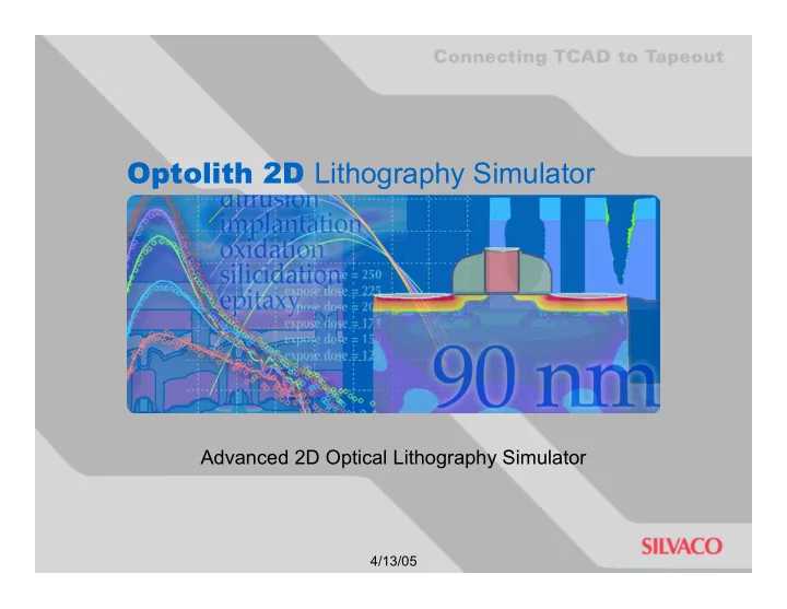
Optolith 2D Lithography Simulator Advanced 2D Optical Lithography - - PowerPoint PPT Presentation
Optolith 2D Lithography Simulator Advanced 2D Optical Lithography Simulator 4/13/05 Introduction Optolith is a powerful non-planar 2D lithography simulator that models all aspects of modern deep sub-micron lithography It provides a fast
4/13/05
Optolith
Optolith
Optolith
4/13/05
Optolith
Optolith
Optolith
Optolith
Optolith
Optolith
Optolith
Optolith
Optolith
Optolith
4/13/05
Optolith
Optolith
Optolith
Optolith
Optolith
Optolith
Optolith
Optolith
Optolith
Optolith
Optolith
Optolith
Optolith
Optolith
Optolith
Optolith
Optolith
Optolith