FABRICATION OF UNIFORM SQUARE-SHAPED TUNNEL PITS BY ELECTROCHEMICAL - - PDF document

fabrication of uniform square shaped tunnel pits by
SMART_READER_LITE
LIVE PREVIEW

FABRICATION OF UNIFORM SQUARE-SHAPED TUNNEL PITS BY ELECTROCHEMICAL - - PDF document

18 TH INTERNATIONAL CONFERENCE ON COMPOSITE MATERIALS FABRICATION OF UNIFORM SQUARE-SHAPED TUNNEL PITS BY ELECTROCHEMICAL ETCHING ON ALUMINUM FOIL H.S Park 1,2 *, N.J Kim 1 , T.Y Kim 1, C.H Lee 1 , J.H Jang 1 , S.J Suh 1,2 1 School of Advanced


slide-1
SLIDE 1

18TH INTERNATIONAL CONFERENCE ON COMPOSITE MATERIALS

1.Introduction Capacitor, one of the most widely electronics components, have been developed for many electronic such as mobile phone, computer and digital appliances. Recently in automotive electronics, the need for high power capacitor increased largely due to the development of hybrid electronic(HEV) and fuel cell vehicle[1-3]. Among the currently existing capacitor, aluminum electrolytic capacitor which has been used for industrial motor inverter application is basically composed of anode foil with dielectric layer of barrier-type anodic aluminum oxide(AAO) and cathode foil with an organic electrolyte-impregnated separator sandwich in between. At aluminum capacitor, As you know, it is important to maximize the surface area of electrode because the capacitance C is directly proportional to the etched aluminum surface area S as well as to the permittivity ε of dielectric oxide, and inversely proportional to the

  • xide thickness d (C= ε S/d)[4-6]. In this work, we

fabricate the uniform tunnel pits and regular intervals and avoiding an excessive dissolution of the Al surface using polyimide materials as Mask

  • layer. The goal of this experiments increase

vertically the aluminum surface area S through the etched tunnel pit on Al foil and was to inspect the controllability of the etching tunnel, and this was confirmed through the selective electrochemical etching with the patterning on aluminum foil.

  • 2. Experimetal

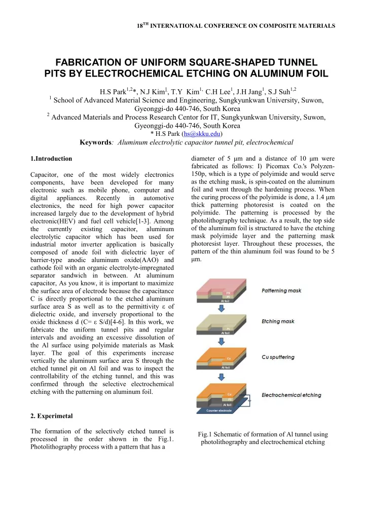
The formation of the selectively etched tunnel is processed in the order shown in the Fig.1. Photolithography process with a pattern that has a diameter of 5 μm and a distance of 10 μm were fabricated as follows: I) Picomax Co.'s Polyzen- 150p, which is a type of polyimide and would serve as the etching mask, is spin-coated on the aluminum foil and went through the hardening process. When the curing process of the polyimide is done, a 1.4 μm thick patterning photoresist is coated on the

  • polyimide. The patterning is processed by the

photolithography technique. As a result, the top side

  • f the aluminum foil is structured to have the etching

mask polyimide layer and the patterning mask photoresist layer. Throughout these processes, the pattern of the thin aluminum foil was found to be 5 μm. Fig.1 Schematic of formation of Al tunnel using photolithography and electrochemical etching

FABRICATION OF UNIFORM SQUARE-SHAPED TUNNEL PITS BY ELECTROCHEMICAL ETCHING ON ALUMINUM FOIL

H.S Park1,2*, N.J Kim1, T.Y Kim1, C.H Lee1, J.H Jang1, S.J Suh1,2

1 School of Advanced Material Science and Engineering, Sungkyunkwan University, Suwon,

Gyeonggi-do 440-746, South Korea

2 Advanced Materials and Process Research Centor for IT, Sungkyunkwan University, Suwon,

Gyeonggi-do 440-746, South Korea

* H.S Park (hs@skku.edu)

Keywords: Aluminum electrolytic capacitor tunnel pit, electrochemical

slide-2
SLIDE 2

After the patterning process of the polyimide etching mask layer on the thin aluminum foil, 1 nm of a thin Cu layer is deposited using sputtering equipment. Finally, the electrochemical etching is conducted on the polyimide etching mask layer and an alumin etching layer that has the selectively formed etching tunnel is made. For the uniformity of the etching tunnels, the current density was selected to be mA/cm2 and the temperature was chosen to be 50 Moreover, the size, the shape of the etching t and process has been studied while controlling the time parameters with 20, 30, 40 and 50 seconds. After electrochemical etching, polyimide etching mask layer on aluminum is removed by etching solutions.

  • 3. Results and Discussion

The effect of electro-polishing produces a uniform tunnel pit as decrease surface roughness in Fig.2, Surface roughness can be decrease around up to 50nm by using electro-polishing conditions The electrochemical etching of high been widely used to produce a large surface area a Al anode for electrolytic capacitors. production of high-voltage electrolytic capacitor, Al foils predominantly composed of the (100) plane etched under a DC condition in chloride chloride-containing electrolyte. produces fine tunnel pits oriented along the <100> direction of Al. Fig.2. Effect of electro-polishing After the patterning process of the polyimide etching mask layer on the thin aluminum foil, 1 nm of a thin Cu layer is deposited using sputtering equipment. Finally, the electrochemical etching is conducted on the polyimide etching mask layer and an aluminum etching layer that has the selectively formed etching tunnel is made. For the uniformity of the etching tunnels, the current density was selected to be 300 and the temperature was chosen to be 50 ºC. Moreover, the size, the shape of the etching tunnel, been studied while controlling the time parameters with 20, 30, 40 and 50 seconds. After electrochemical etching, polyimide etching mask layer on aluminum is removed by etching polishing produces a uniform as decrease surface roughness. As shown Surface roughness can be decrease around polishing conditions. e electrochemical etching of high-purity Al has to produce a large surface area on a Al anode for electrolytic capacitors. For the voltage electrolytic capacitor, Al foils predominantly composed of the (100) plane is etched under a DC condition in chloride-condition in ing electrolyte. This process produces fine tunnel pits oriented along the <100> polishing. A Picomax Polyzen-150p polyimide is used for the etching mask due to its strong resistance against acid. However, because the Polyzen photosenstive polyimide, after the polyimide is coated, a separate patterning of the photoresist should be performed. Fig. images of photo lithography after PR removal. Fig.3. Plane-view SEM images of photo lithography after PR removal : polyimide / aluminum foil Fig.4 shows the surface state containing the aluminum pit resulted from the removal of the polyimide on the aluminum foil. Fig.4 Plane-view SEM images of etch ºC/300 mA/cm2 after polyimide removal 30’s (c) 40’s (d) 50’s By inspecting the images of the aluminum foil processed for 20, 30, 40 and 50 seconds captured by the electron microscopy, one can se has little loss and uniform etching tunnels have been 150p polyimide is used for the etching mask due to its strong resistance against acid. However, because the Polyzen-150p is a non- photosenstive polyimide, after the polyimide is coated, a separate patterning of the photoresist Fig.3 is plane-view SEM images of photo lithography after PR removal. view SEM images of photo lithography after PR removal : polyimide / aluminum foil shows the surface state containing the aluminum pit resulted from the removal of the polyimide on the aluminum foil. view SEM images of etch tunnel at 50 after polyimide removal: (a) 20’s (b) By inspecting the images of the aluminum foil processed for 20, 30, 40 and 50 seconds captured by the electron microscopy, one can see that the surface has little loss and uniform etching tunnels have been

slide-3
SLIDE 3

formed in the images (a) and (b). On the other hand, in the images (c) and (d), one can observe that the loss of the surface starts to appear. deep the tunnels are etched, the sample was cut such that the cross section is exposed, and the depth of the etching tunnel was measured. Fig.5 images showing the etching depth of the aluminum for etching times of 20, 30, 40, and can be seen in the images (a) and (b), the initial growth of the electrochemical etching of the aluminum foil is kept vertically in cubical shapes. On the other hand, as can be seen in the images (c) and (d), although the diameter of the bot does not show a big difference from the images (a) and (b), when the etching tunnel is longer, the diameter becomes narrower as it goes deeper into the film. In other words, (the fact that the tunnel becomes narrower as the etching tunnel grows means that) the resistance of the electrolyte increases due to the space formed between the outside of the tunnel and the cross section of the corroded tunnel. Hence, the corroding rate of the chlorine ions is reduced and the corroded area is diminished, and this results in overall decrease of size of the tunnel pits toward the etching direction. As the etching proceeds deep enough into the aluminum foil, the influence of the current density become smaller at the sites where the texturing is not well the rolling process, and we believe that this results in a loss of the directionality of the etching process. Fig.5. Plane-view SEM images of etch depth : (a) 20 sec (b) 30 sec (c) 40 sec (d) 50 sec formed in the images (a) and (b). On the other hand, in the images (c) and (d), one can observe that the loss of the surface starts to appear. To know how deep the tunnels are etched, the sample was cut such that the cross section is exposed, and the depth of the is microscope images showing the etching depth of the aluminum 50 seconds. As can be seen in the images (a) and (b), the initial growth of the electrochemical etching of the aluminum foil is kept vertically in cubical shapes. On the other hand, as can be seen in the images (c) and (d), although the diameter of the bottom part does not show a big difference from the images (a) and (b), when the etching tunnel is longer, the diameter becomes narrower as it goes deeper into the film. In other words, (the fact that the tunnel becomes narrower as the etching tunnel grows ans that) the resistance of the electrolyte increases due to the space formed between the outside of the tunnel and the cross section of the corroded tunnel. Hence, the corroding rate of the chlorine ions is reduced and the corroded area is diminished, and this results in overall decrease of size of the tunnel pits toward the etching direction. As the etching proceeds deep enough into the aluminum foil, the influence of the current density become smaller at the sites where the texturing is not well-formed from the rolling process, and we believe that this results in a loss of the directionality of the etching process. view SEM images of etch depth : (a) 20 Resultingly, as can be seen from Fig. depth increases continuously from 15 μm for after initial 20 seconds to 36 μm when passed.

10 20 30 10 15 20 25 30 35 40

Tunnel Depth(um) Time(sec)

Tunnel Depth Curve for Current Density 300mA/cm

Fig.6. Tunnel depth curve for current density 400mA However, as the etching depth is being deeper as shown in the Fig.6 (d), the width of the etching tunnel becomes narrow. To solve this problem, changing current density step by step over time might be necessary.

  • 4. Conclusion

In this experiment, a research increase the capacitance of the aluminum capacitor, which has been spotlighted for its rapid development into electronic components. The goal of this experiment was to inspect the controllability of the etching tunnel, and this was confirm selective electrochemical etching with the patterning

  • n aluminum foil. To find out the best patterning

conditions on the aluminum foil, various patterning techniques had been tried, and the photolithography was found to give the best result for the patterning method. To acquire the condition for uniform etching of the patterned aluminum foil, current density and electrolyte temperature were kept constant while the etching time was being changed to find out the optimal condit

  • ptimize the number of defect sites and the

condition of distribution, which would act as the corrosion starting points during the electrochemical etching process, the trace of the fluid used during the

3 PAPER TITLE

Resultingly, as can be seen from Fig. 6, the etching depth increases continuously from 15 μm for after initial 20 seconds to 36 μm when 50 seconds have

40 50 60

Time(sec)

Tunnel Depth Curve for Current Density 300mA/cm

2

l depth curve for current density 400mA However, as the etching depth is being deeper as (d), the width of the etching tunnel becomes narrow. To solve this problem, changing current density step by step over time In this experiment, a research was performed to increase the capacitance of the aluminum capacitor, which has been spotlighted for its rapid development into electronic components. The goal of this experiment was to inspect the controllability of the etching tunnel, and this was confirmed through the selective electrochemical etching with the patterning

  • n aluminum foil. To find out the best patterning

conditions on the aluminum foil, various patterning techniques had been tried, and the photolithography was found to give the best result and was selected for the patterning method. To acquire the condition for uniform etching of the patterned aluminum foil, current density and electrolyte temperature were kept constant while the etching time was being changed to find out the optimal condition. To

  • ptimize the number of defect sites and the

condition of distribution, which would act as the corrosion starting points during the electrochemical etching process, the trace of the fluid used during the

slide-4
SLIDE 4

rolling process and the oil film on the rolled aluminum foil were removed. however, by inspecting the shape of the etched fits on the surface, it was found out that although the distribution of etching tunnels is uniform as the current density increases, if the current density exceeds its threshold values, excessive concentration of current occurs, resulting in the etching mask detachment and some consequent surface corrosions due to the high current density. Throughout these tests, 400mA/cm2 was found to be the best condition for that the diameter of the etching tunnel is not much reduced from the original patterning size and the etching tunnels are formed uniformly on the surface.

References [1] W.J. Sarjeant, J.Zirnheld, etc, Handbook of Low and High Dielectric Constant Materials and Their Application, Academic, London, 1999 [2] A. Nishino, J. Power Source 60(1996) 137 [3] T. Efford, Y.Shibata, S. Ando, A. Kanezaki, IEEE Industry Application Society (1997) [4] Tatsuro Fukushima, kazuyuk Nishio, and Hideki Masuda, Electrochemical and Solid- State Letters, 13(4) C9-C11(2010). [5] Sachiko Ono, kota Uchibori and Hidetaka Asoh, Surf. Interface Anal., 2010,42,264-268 [6] K.Hebert and R.Alkire, J. Electrochem. Soc., 135, 2146(1998)