
SLIDE 1
1
jlee1@uamail.albany.edu
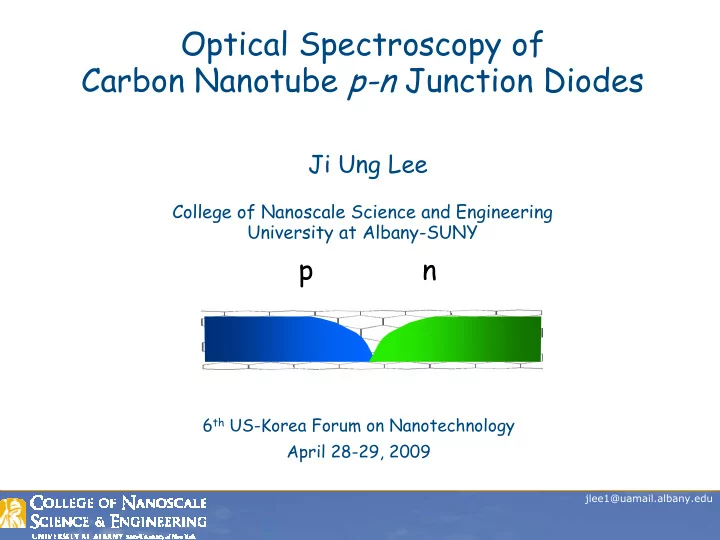
Optical Spectroscopy of Carbon Nanotube p-n Junction Diodes
Ji Ung Lee
College of Nanoscale Science and Engineering University at Albany-SUNY
6th US-Korea Forum on Nanotechnology April 28-29, 2009
Optical Spectroscopy of Carbon Nanotube p-n Junction Diodes Ji Ung - - PowerPoint PPT Presentation
Optical Spectroscopy of Carbon Nanotube p-n Junction Diodes Ji Ung Lee College of Nanoscale Science and Engineering University at Albany-SUNY p n 6 th US-Korea Forum on Nanotechnology April 28-29, 2009 jlee1@uamail.albany.edu 1 The College
1
jlee1@uamail.albany.edu
6th US-Korea Forum on Nanotechnology April 28-29, 2009
2
jlee1@uamail.albany.edu
3
jlee1@uamail.albany.edu
4
jlee1@uamail.albany.edu
ANT/CNSE will house over 125 state-of-the-art 300mm wafer tools when build out is completed. Designed for 32nm node & beyond but compatible with previous generations.
capability.
by partners. Facility capable of 25 integrated wafer starts (WSD) per day.
5
jlee1@uamail.albany.edu
70nm 70nm
6
jlee1@uamail.albany.edu
7
jlee1@uamail.albany.edu
8
jlee1@uamail.albany.edu
EC EV EF
EC EV
N-type(electrons) P-type(holes)
EC EV 1 2 3
9
jlee1@uamail.albany.edu
J.U. Lee et. al., APL: July 5, 2004
10
jlee1@uamail.albany.edu
11
jlee1@uamail.albany.edu
J.U. Lee et. al., APL: July 5, 2004
0 100 5 10-7 1 10-6
0.5 1 1.5
V
DS(Volts)
+10V +10V
12
jlee1@uamail.albany.edu
T nK qV
10 -11 10 -10 10 -9 10 -8 10 -7
0.2 0.4
VGS1,2=+/-10V Fit V
DS (Volts)
13
jlee1@uamail.albany.edu
10 -11 10 -10 10 -9 10 -8 10 -7
0.2 0.4
V
DS (Volts)
14
jlee1@uamail.albany.edu
(a) (b) 1 µm
15
jlee1@uamail.albany.edu
10
10
10
10
10
10
10
0.5 1
Fit Data
1.E-13 1.E-12 1.E-11 1.E-10 1.E-09 1.E-08 1.E-07
0.5
J.U. Lee, Appl. Phys. Lett. 87, 073101 (2005)
16
jlee1@uamail.albany.edu
4x10 -12 8x10 -12
0.1
Voc and Isc: Completely define PV properties for an ideal diode
J.U. Lee, Appl. Phys. Lett. 87, 073101 (2005)
17
jlee1@uamail.albany.edu
0.00 0.05 0.10 10
10
10
10
10
IDS (A) VDS(V)
(similar to SWNTs in solution)
0.5 1.0 1.5 1x10
2x10
3x10
4x10
ISC (A) Energy (eV)
1 2 3 4 5
J.U. Lee et.al., Appl. Phys. Lett. 90, 053103 (2007)
18
jlee1@uamail.albany.edu
3D Bulk Semiconductor 2D Quantum Well 1D Quantum Wire 0D Quantum Dot
E
E E E
19
jlee1@uamail.albany.edu
Exciton Hydrogenic Levels n=1,2,3… continuum
20
jlee1@uamail.albany.edu
E
21
jlee1@uamail.albany.edu
22
jlee1@uamail.albany.edu
EB 2 3 = E22 1 = E11
Lack of any features at Eg due to Sommerfeld factor <1 Side bands measure dark exciton
J.U. Lee et.al., Appl. Phys. Lett. 90, 053103 (2007)
23
jlee1@uamail.albany.edu
1.0 1.2 1.4 1.6 1.8 2.0 0.4 0.8 1.2 1.6 2.0
100 200 300
Intensity (a.u.) Raman frequency (cm
+: Emperical Kataura Weisman et.al. Nano Lett. 3, 1235 (2003)
– Exciton-phonon ▲ - Quasipaticle Bandgap
24
jlee1@uamail.albany.edu
0.4 0.5 0.6 0.5 0.6 0.7 0.8 0.9 1.0
0.5 1.0 1.5 10 20 30 40
4 1 = E11 2 ISC (fA) Energy (eV) 3 = E22 5 = E33
E11 (eV) Ea(eV) E11=Ea
0.00 0.05 0.10 0.15 0.20 10
10
10
10
10
10
10
10
IDS (A) VDS (V)
25
jlee1@uamail.albany.edu
D
pn np
S
E11
1 2 3
EB Ea
L
EF EC EV Ea
J.U. Lee, Phys. Rev. B 75, 075409 (2007)
26
jlee1@uamail.albany.edu
0.00 0.05 0.10 0.15 0.20 1E-15 1E-14 1E-13 1E-12 1E-11 1E-10 1E-9 1E-8 6V 8V 11V
IDS (A) VDS (V)
SiO2
VG1 VG2 S D
L
27
jlee1@uamail.albany.edu
Minority Carriers
No shrinkage
band gap Shrinkage
band gap
28
jlee1@uamail.albany.edu
29
jlee1@uamail.albany.edu
Split Gates Split Gates 1,2...layer 1,2...layer graphene graphene flake flake
n n-
type p p-
type n n-
type p p-
type