<<< back | overview | next >>>
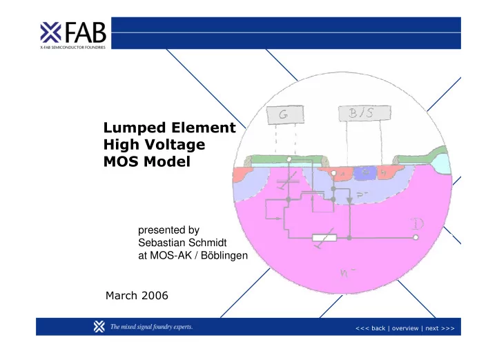
Lumped Element High Voltage MOS Model presented by Sebastian - - PowerPoint PPT Presentation
Lumped Element High Voltage MOS Model presented by Sebastian Schmidt at MOS-AK / Bblingen March 2006 <<< back | overview | next >>> Devices DC Model AC Model Test Bench Outlook Agenda (1) > > The Devices:
<<< back | overview | next >>> 2
Devices DC Model AC Model Test Bench Outlook
> The Devices:
Types and Construction
> DC Model:
Mathematical considerations, types
> AC Model:
Non diode variable "gate" capacitance
> Ring Oscillator Test Bench:
A challenge for the simulator
> Outlook
Agenda (1)
>
<<< back | overview | next >>> 3
Devices DC Model AC Model Test Bench Outlook
Introduction
> The goal is to show an extension to the BSIM3v3 model
which can be simulated by a standard Spice simulator.
> At the time of development a VerilogA formulation was
not intended.
> The model shows a more accurate description of the so
called quasi saturation effect.
> A better description of the LDDMOS drain overlap
capacitance is considered.
<<< back | overview | next >>> 4
Devices DC Model AC Model Test Bench Outlook
High Voltage Drain Extension MOS Cross Section
- 1E20
- 1E18
- 1E16
- 1E14
- 1E12
N-WELL P-WELL
BULK GATE DRAIN SOURCE
P-SUB
Si depth / µm position / µm
watch the scaling
<<< back | overview | next >>> 5
Devices DC Model AC Model Test Bench Outlook
Two Types of Drain Extension MOS
Extension region at drain Circuit with drain resistance and parasitic elements (BJT, substrate resistance) Name: Extended Drain MOS XDMOS N-Well as drain extension
<<< back | overview | next >>> 6
Devices DC Model AC Model Test Bench Outlook
Two Types of Lateral Diffused Drain MOS
Diffused drain with lateral drain connection Name: LDDMOS
- r LDMOS
Diffused drain with vertical drain connection XD_10 with up to 650 V LDMOS transistors Trench
<<< back | overview | next >>> 7
Devices DC Model AC Model Test Bench Outlook
> The Devices:
Types and Construction
> DC Model:
Mathematical considerations, types
> AC Model:
Non diode variable "gate" capacitance
> Ring Oscillator Test Bench:
A challenge for the simulator
> Outlook
Agenda (2)
>
<<< back | overview | next >>> 8
Devices DC Model AC Model Test Bench Outlook
First Generation HV MOS Model
> MOS transistor with serial resistor
- good model accuracy for low gate voltages
- drain current saturation effect at high VGS and VDS not included
- fast simulation speed and good convergence
MOS BSIM3V3 Rds D G S
VGS/V 12.0 9.67 7.33 5.0 2.67
The model does not take into account the quasi saturation effect.
<<< back | overview | next >>> 9
Devices DC Model AC Model Test Bench Outlook
VGS/V 12.0 9.67 7.33 5.0 2.67
Second Generation Behavioural HV MOS
- core devices MOS and Rds identical to HV model
- several parameters for VCVS added
- good model accuracy, error less than 10%
- higher simulation time
- simulation convergence problems more likely
> MOS transistor with serial resistor and
voltage controlled voltage source
D G S Rds MOS BSIM3V3
The quasi saturation is modeled with acceptable accuracy (green).
<<< back | overview | next >>> 10
Devices DC Model AC Model Test Bench Outlook
Function Requirement for the Voltage Source
> Demands on the behavioral current function:
– The function should be monotone (not necessarily). – The first and second derivative must be continuous.
Voltage drop @ resistor.
Rd Function Function needed for the voltage source:
<<< back | overview | next >>> 11
Devices DC Model AC Model Test Bench Outlook
Implementation: Controlled Voltage Source
> Auxiliary Networks:
evd = max(sgn(v(d,s)),0) * max(sgn(v(g,s)),0) * min(v(7)*v(6),v(d,s))
> Improved accuracy has its price:
3 auxiliary networks, 7 parameters, several additional elements TC network 7 R=1k tc1=5.5E-3 tc2=1.2E-5 ev = ( kp3 v(5)3 + kp4 v(5)4 + kp5 v(5)5 ) * f(v(g,s),k1h,kgs) * flimit(v(d,s),kds)
+
- d
9 8 g s b evd 1f Rd ev
+
- 6
main formula 1M
+
- 5
ev5 = v(d,9) / ( v(7) + 1E-6 ) ev5 1M
<<< back | overview | next >>> 12
Devices DC Model AC Model Test Bench Outlook
Current Source Behavioural HV MOS
- core devices MOS and Rds identical to HV model
- added fly back diode due to device construction
- improved accuracy compared to the voltage source model
- shorter simulation time
- capacitance modeling difficult in case of LDDMOS
1 11 12 3 2 BSIM3v3
> MOS transistor with serial resistor and
voltage controlled current source
<<< back | overview | next >>> 13
Devices DC Model AC Model Test Bench Outlook
Function Requirements for the Current Source
The function for the current in the drain extension region Variations ... Resulting resistance must
<<< back | overview | next >>> 14
Devices DC Model AC Model Test Bench Outlook
Behavioural Current Source Model
> Less auxiliary sources, improved TC modeling. > More compact model, all effects in a few equations. > Improved convergence, fewer parameter (5).
g11 3 1G 1f R01 tc1' tc2' s d g 2 12 1 11 TC 102 R=1 tc1,tc2 I=R02 101 1 Gate Voltage influence: I=f(v(2,3),a,b,c) * v(102) 1+ v(11,12)2 / v(101)2 I(g11) = v(11,12) v(102) * 1+
<<< back | overview | next >>> 15
Devices DC Model AC Model Test Bench Outlook
Gm and Transconductance Example
Id [1E-3] red: measured green: simulated
<<< back | overview | next >>> 16
Devices DC Model AC Model Test Bench Outlook
Gds and Ron accuracy
Gds.m Gds.s [E-3] Ron.m Ron.s [E+0]
<<< back | overview | next >>> 17
Devices DC Model AC Model Test Bench Outlook
Self Heating
> The below plot shows clear self heating:
a "falling" current trace in the saturation region
> To include this effect into the model, it needs a
temperature node and additionaly ...
> A thermal resistance / capacitance network.
It's not yet implemented in the model.
<<< back | overview | next >>> 18
Devices DC Model AC Model Test Bench Outlook
Introduction to Self Heating
> Simple thermal network added for self heating:
– Voltage [V] = Temperature [K] – Current [I] = Thermal Current [J/s=W] – Resistance [Ω] = Thermal Resistance [K/W] – Capacitance [C/V] = Thermal Capacitance [J/K] – Charge [C] = Energy [J=Ws]
> The thermal power equals the electrical power loss.
^ ^ ^ ^ ^
+
- Ambient
Temperature Thermal Network Rth-out Cth-out
+
- Pel-loss = Ithermal
Device Temperature 1G Cth-Dev Rth-Dev Thermal Node: this voltage goes into the formulas as temperature. T=Vth
<<< back | overview | next >>> 19
Devices DC Model AC Model Test Bench Outlook
> The Devices:
Types and Construction
> DC Model:
Mathematical considerations, types
> AC Model:
Non diode variable "gate" capacitance
> Ring Oscillator Test Bench:
A challenge for the simulator
> Outlook
Agenda (3)
>
<<< back | overview | next >>> 20
Devices DC Model AC Model Test Bench Outlook
- 1E20
- 1E18
- 1E16
- 1E14
- 1E12
P-WELL N-WELL Si depth / µm position / µm
BULK/SOURCE GATE DRAIN
The Drain Overlap Capacitance Problem
- 1E20
- 1E18
- 1E16
- 1E14
- 1E12
P-WELL N-WELL Si depth / µm position / µm
BULK/SOURCE GATE DRAIN
A capacitance, which depends strongly from the drain voltage, develops if the gate
- verlaps the drain
extension region. This is true for the LDDMOS type MOS with Trench isolation. Fortunately it does not occur in the standard CMOS technologies, e.g. xc06.
<<< back | overview | next >>> 21
Devices DC Model AC Model Test Bench Outlook
LDDMOS Capacitance Model
> For the LDDMOS of the XD?10 technology a (variable)
capacitance has to be added in the drain to gate path.
> It can not be decided by CV measurement which node has
to be occupied to get a good fitting transient respond. D
1 11 12 3 2 BSIM3v3
? ? ?
<<< back | overview | next >>> 22
Devices DC Model AC Model Test Bench Outlook
Improved CV Model
This model is not yet implemented in X-FAB's HV models, ongoing work. constant cap @ drain (purple) improved model (green)
this is the reverse diode, which is easily modeled drain overlap w/o channel This is the drain/gate
- verlap capactance,
which has a diode like CV trace
<<< back | overview | next >>> 23
Devices DC Model AC Model Test Bench Outlook
Drain Voltage dependent Capacitance Model
> The capacitance is modeled in an
auxiliary circuit. The current is mirrored back into the current controlled current source between the drain and gate node.
> This is fine for stand alone AC
simulation but proved as not converging in the ring oscillator test. An alternative model is in development. It uses function controlled sources instead of diodes to modulate the CV characteristic. g g11 3 1G 1f R01 Cgd1 s d 2 12 1 11 Icgd
+
- +
- V=v(2,1)
0V Icgd 1 1 Dcgd Cgd2 Cgd D2 D1 accumulating constant part
<<< back | overview | next >>> 24
Devices DC Model AC Model Test Bench Outlook
> The Devices:
Types and Construction
> DC Model:
Mathematical considerations, types
> AC Model:
Non diode variable "gate" capacitance
> Ring Oscillator Test Bench:
A challenge for the simulator
> Outlook
Agenda (4)
>
<<< back | overview | next >>> 25
Devices DC Model AC Model Test Bench Outlook
Health Checks and Convergence Tests
> The Model is tested regarding convergence. > DC check with extended voltages. > Transient analysis with ring oscillator as benchmark.
I will show two bad examples from the time of model development
- n the next slides ...
Simulation health check with high gate and drain voltages:
<<< back | overview | next >>> 26
Devices DC Model AC Model Test Bench Outlook
Behavioural Model Pitfalls (1):
0.00 0.05 0.10 0.15 0.20 0.25 20 40 60 80 100 Vd [V] Id [A] .dc Vd 0 100 1 Vg list 3 4 5 6 7 8 0.00 0.05 0.10 0.15 0.20 0.25 0.30 0.35 2 4 6 8 10 12 14 16 Vg [V] Id [A] .dc Vg 0 15 0.2; Vd=50
Adverse effect of high drain voltage
- n the effective gate voltage:
The model is not physical. Initially the model was extracted at low gate / drain voltages. It was not sanity checked.
<<< back | overview | next >>> 27
Devices DC Model AC Model Test Bench Outlook
Behavioural Model Pitfalls (2):
MDH08
- 1.00
- 0.50
0.00 0.50 1.00 1.50 100 200 300 400 Vd [V] Id [A] .dc Vd 0 450 1 Vg 5 20 5
Negative drain current in the simulation due to a reversed voltage in the drain voltage
- source. This can occur if
the mathematical formulation is not monotone or no cautions are taken against nonphysical results. The simulator finds convergence even with the impossible ...
> Non physical convergence found by the simulator:
<<< back | overview | next >>> 28
Devices DC Model AC Model Test Bench Outlook
.option tnom=27 gmindc=1e-16 gmin=1e-16 pivtol=0.5e-16 .option newtol ingold=1 absi=1e-10 reli=1e-5 relv=1e-4 .option nomod .TEMP 27.00 * Analyses .tran 1n 50n uic .print tran v(1) .param vdd = 15 vvdd vdd 0 'vdd'
.ic v(1)='vdd' * Initial Condition to * start the oscillation
.subckt inv i o vdd xmp o i vdd vdd phve w=40u l=3.5u pd=50u ps=50u ad=160p as=40p nrd=0.025 nrs=0.025 xmn o i 0 0 nhve w=20u l=3.5u pd=30u ps=30u ad=80p as=20p nrd=0.025 nrs=0.025 .ends inv .subckt inv8 1 9 vdd xi1 1 2 vdd inv xi2 2 3 vdd inv
. . . .
xi6 6 7 vdd inv xi7 7 8 vdd inv xi8 8 9 vdd inv .ends inv8 xinv1 1 2 vdd inv8
. . . .
xinv3 3 4 vdd inv8 xinv0 4 1 vdd inv
Ringoscillator Test Circuitry
> Ring oscillator with 25 stages
In this case NMOS and PMOS HV model. Alternative if only NMOS (PMOS respective):
<<< back | overview | next >>> 29
Devices DC Model AC Model Test Bench Outlook
Transient Analysis Test Bench Results
Factor 15 to >50 depending on mathematics behind the model. The challenge is the transient analysis. AC and DC analyses are more robust regarding convergence. not converg. Model with CV modelling (diodes) 40.24 Final Behavioural Current Source Model 47.94 Improved Model, changed maths 133.35 First Current Source Model 36.41 Resistor with behavioural voltage source 2.52 Simple resistor @ drain CPU time [s] Model Type
> The transient analysis simulation time is considerably
longer compared to the simple resistor model.
<<< back | overview | next >>> 30
Devices DC Model AC Model Test Bench Outlook
> The Devices:
Types and Construction
> DC Model:
Mathematical considerations, types
> AC Model:
Non diode variable "gate" capacitance
> Ring Oscillator Test Bench:
A challenge for the simulator
> Outlook
Agenda (5)
>
<<< back | overview | next >>> 31
Devices DC Model AC Model Test Bench Outlook
Plans for Enhancement of the HV Model
> Improvement of the Capacitance Model. > Test of Capacitance and Reverse Diode Model with
transient measurement and simulation. (TT problem)
> Further simplification of the mathematical description
for better convergence.
> Consideration of self heating effects. > Why not VerilogA ?
Most of the Simulators cope with it nowadays. It would made the formulation much simpler.
<<< back | overview | next >>> 32
Devices DC Model AC Model Test Bench Outlook
> The Devices:
Types and Construction
> DC Model:
Mathematical considerations, types
> AC Model:
Non diode variable "gate" capacitance
> Ring Oscillator Test Bench:
A challenge for the simulator
> Outlook
Agenda (6)
>
<<< back | overview | next >>> 33
Devices DC Model AC Model Test Bench Outlook
Acknowledgements
I would like to thank:
> Uta Kuniß (X-FAB)
for countless TCAD simulations.
> Axel Hammer (X-FAB)
for all the help in understanding models.
> Matthias Franke (X-FAB)
for the voltage dependent capacitance model
> In memoriam of my father
who gave me a marvellous start doing physics. as well as ...
> all contributors (elsewhere) providing bits and pieces.
and ...
> Susanne (home), who is sustaining my life.
<<< back | overview | next >>> 34
Devices DC Model AC Model Test Bench Outlook