
Digital Systems Tranmission Lines V CMPE 650 1 (3/18/08)
UMBC
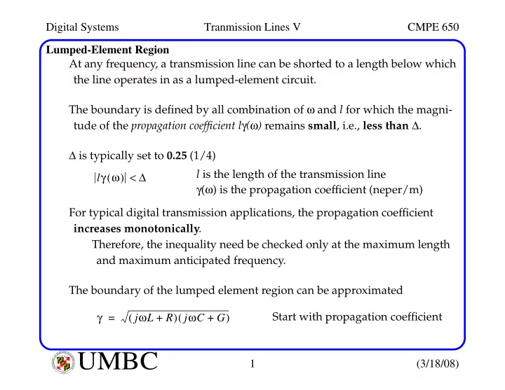
U M B C U N I V E R S I T Y O F M A R Y L A N D B A L T I M O R E C O U N T Y 1 9 6 6Lumped-Element Region At any frequency, a transmission line can be shorted to a length below which the line operates in as a lumped-element circuit. The boundary is defined by all combination of ω and l for which the magni- tude of the propagation coefficient lγ(ω) remains small, i.e., less than ∆. ∆ is typically set to 0.25 (1/4) For typical digital transmission applications, the propagation coefficient increases monotonically. Therefore, the inequality need be checked only at the maximum length and maximum anticipated frequency. The boundary of the lumped element region can be approximated lγ ω ( ) ∆ < l is the length of the transmission line γ(ω) is the propagation coefficient (neper/m) γ jωL R + ( ) jωC G + ( ) = Start with propagation coefficient