Lecture 9 Logistics HW2 due now HW3 due Monday HW3 due Monday - - PDF document

lecture 9
SMART_READER_LITE
LIVE PREVIEW

Lecture 9 Logistics HW2 due now HW3 due Monday HW3 due Monday - - PDF document

Lecture 9 Logistics HW2 due now HW3 due Monday HW3 due Monday Lab --- stay on track Tuesday review 6pm(ish) place TBD Nikhils office hour location moved: CSE 218 same time (M1:30) Last lecture


slide-1
SLIDE 1

Lecture 9

Logistics

HW2 due now HW3 due Monday HW3 due Monday Lab --- stay on track Tuesday review 6pm(ish) place TBD Nikhil’s office hour location moved: CSE 218 same time (M1:30)

Last lecture

"Switching-network" logic blocks

Multiplexers and Demultiplexers

1

CSE370, Lecture 11

Today

PLDs

PLAs PALs

ROMs 9

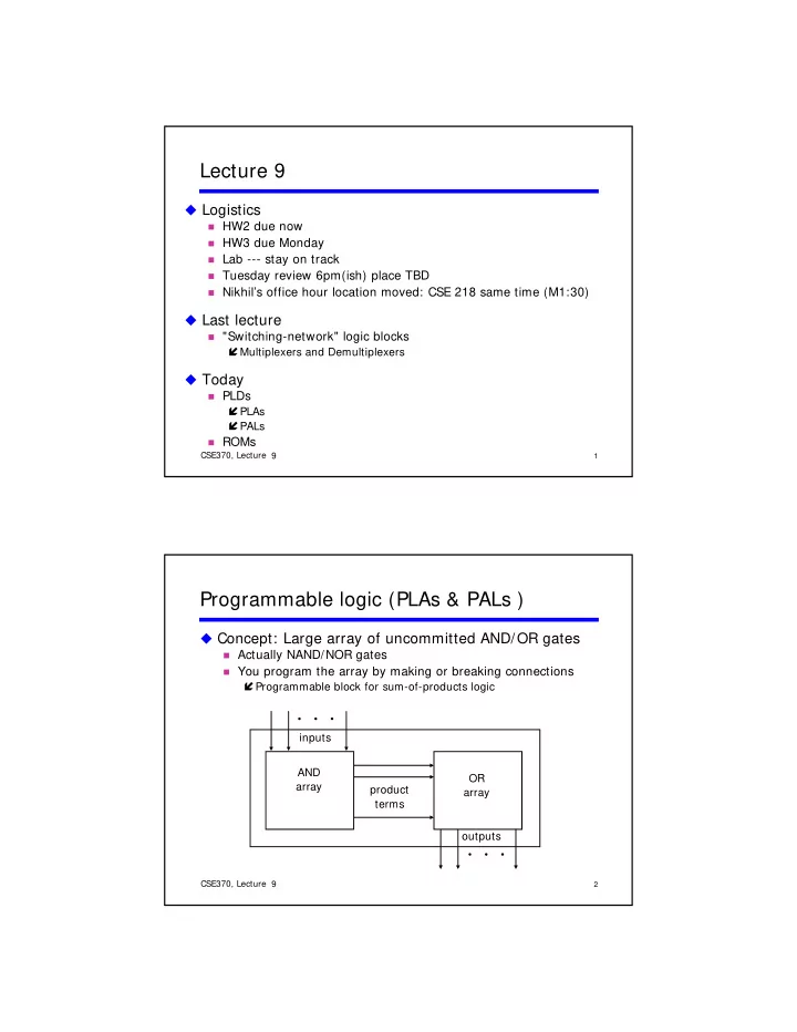
Programmable logic (PLAs & PALs )

Concept: Large array of uncommitted AND/OR gates

Actually NAND/NOR gates You program the array by making or breaking connections

  • • •

inputs product AND array OR

You program the array by making or breaking connections

Programmable block for sum-of-products logic

2

CSE370, Lecture 11

  • • •
  • utputs

product terms array array

9

slide-2
SLIDE 2

Programming the wire connections

Fuse: Comes connected; break unwanted connections Anti-fuse: Comes disconnected; make wanted connections A B C A B C AB B'C AC'

F0 = A + B'C' F1 = AC' + AB F2 = B'C' + AB F3 = B'C + A

3

CSE370, Lecture 11

F1 F2 F3 F0 B'C' A 1

9

Short-hand notation

Draw multiple wires as a single wire or bus ×

signifies a connection After Programming

AB A'B' CD' A B C D

Before Programming

4

CSE370, Lecture 11

F0 F1 C'D

F0 = AB + A'B' F1 = CD' + C'D

9

slide-3
SLIDE 3

A B C

Think of as a memory-address decoder Memory bits

PLA example

F1 = ABC F2 = A + B + C F3 = A' B' C'

A B C F1 F2 F3 F4 F5 F6 0 0 0 1 1 0 0 1 1 0 1 1 1 0 1 0 1 1 1 1 A'B'C' A'B'C A'BC' A'BC AB'C' AB'C

F3 = A B C F4 = A' + B' + C' F5 = A xor B xor C F6 = A xnor B xnor C

5

CSE370, Lecture 11

0 1 0 0 1 1 1 1 0 1 1 1 1 1 0 0 1 1 1 1 1 0 1 1 1 1 1 0 0 1 1 1 1 1 1 1 1 1 ABC' ABC F1 F2 F3 F4 F5 F6

9

PLAs versus PALs

We've been looking at PLAs

Fully programmable AND / OR arrays

Programmable array logic (PAL)

Programmable AND array OR array is prewired

Cheaper and faster than PLAs

6

CSE370, Lecture 11 9

slide-4
SLIDE 4

00 X 1 00 1 X

Example: BCD to Gray code converter

A B C D W X Y Z 1 1 1 1 1

A AB CD 00 01 11 10 A AB CD 00 01 11 10 01 1 X 1 11 1 X X 10 1 X X 01 1 X 11 X X 10 X X 00 X 1

1 1 1 1 1 1 1 1 1 1 1 1 1 1 1 1 1 1 1 1 1 1 1 1 1 1 1 1 1 1 1 1 X X X X 1 1 1 X X X X 1 1 X X X X 1 1 1 X X X X

D C B K-map for W D C B A 00 1 X AB CD 00 01 11 10 A AB CD 00 01 11 10 K-map for X

7

CSE370, Lecture 11 01 1 X 11 1 X X 10 1 X X

1 1 1 X X X X 1 1 1 1 X X X X

D 01 1 X 11 1 1 X X 10 1 1 X X C B D C B K-map for Y K-map for Z 9

Example: BCD to Gray --- Wire a PLA

A B C D

Minimized functions: W = A + BC + BD X = BC' X = BC Y = B + C Z = A'B'C'D + BCD + AD' + B'CD'

8

CSE370, Lecture 11

W X Y Z

9

slide-5
SLIDE 5

Example: Wire a PAL

Minimized functions: W = A + BC + BD X = BC' X = BC Y = B + C Z = A'B'C'D + BCD + AD' + B'CD’ Fine example for the use of PAL (because no shared AND terms)

9

CSE370, Lecture 11

Many AND gates wasted, but still faster and cheaper than PLA

9

Compare implementations for this example

PLA:

No shared logic terms in this example 10 decoded functions (10 AND gates) 10 decoded functions (10 AND gates)

PAL:

Z requires 4 product terms

16 decoded functions (16 AND gates) 6 unused AND gates

This decoder is a best candidate for PLAs/PALs

10 of 16 possible inputs are decoded

10

CSE370, Lecture 11 10 of 16 possible inputs are decoded No sharing among AND terms

Another option?

Yes — a ROM 9

slide-6
SLIDE 6

Read-only memories (ROMs)

Two dimensional array of stored 1s and 0s

Input is an address ⇒ ROM decodes all possible input addresses Stored row entry is called a "word" ROM output is the decoded word

inputs n address lines

n

  • • •

memory array

11

CSE370, Lecture 11

  • utputs

2n word lines decoder

  • • •

array (2n words by m bits)

9

ROM details

Similar to a PLA but with a fully decoded AND array Completely flexible OR array (unlike a PAL) Extremely dense: One transistor per stored bit Extremely dense: One transistor per stored bit decoder 2n-1 +5V 1 2

Only one word line is active at any time

12

CSE370, Lecture 11

0 n-1 Address

Bit lines: Normally pulled high through

  • resistor. If transistor stores a zero, then

line pulls low when row is selected

m-1 Outputs

9

slide-7
SLIDE 7

Two-level combinational logic using a ROM

Use a ROM to directly store a truth table

No need to minimize logic Example:

F0 = A'B'C + AB'C' + AB'C

A B C F0 F1 F2 F3 0 0 0 1 0 0 1 1 1 1 ROM 8 words x 4 bits/word Example:

F0 = A B C + AB C + AB C F1 = A'B'C + A'BC' + ABC F2 = A'B'C' + A'B'C + AB'C' F3 = A'BC + AB'C' + ABC'

You specify whether to store 1 or 0 in each

13

CSE370, Lecture 11

0 1 0 1 0 1 1 1 1 0 0 1 1 1 1 0 1 1 1 1 0 1 1 1 1 1 8 words x 4 bits/word address

  • utputs

A B C F0 F1 F2 F3

location in the ROM

9

ROMs versus PLAs/PALs

ROMs

Benefits

Quick to design simple dense Quick to design, simple, dense

Limitations

Size doubles for each additional input Can't exploit don't cares

PLAs/PALs

Benefits

Logic minimization reduces size PALs faster/cheaper than PLAs

14

CSE370, Lecture 11

PALs faster/cheaper than PLAs

Limitations

PAL OR-plane has hard-wired fan-in

Another alternative: Field programmable gate arrays

Learn a bit more later in this class 9

slide-8
SLIDE 8

Example: BCD to 7-segment display controller

The problem

Input is a 4-bit BCD digit (A, B, C, D) Need signals to drive a display (7 outputs C0

C6)

c0 c1 c2 c3 c4 c5 c6

c1 c5 c2 c4 c6 c0 c3 Need signals to drive a display (7 outputs C0 – C6)

15

CSE370, Lecture 11

BCD to 7–segment control-signal decoder

A B C D

9

A B C D C0 C1 C2 C3 C4 C5 C6 1 1 1 1 1 1

Formalize the problem

Truth table

Many don’t cares 1 1 1 1 1 1 1 1 1 1 1 1 1 1 1 1 1 1 1 1 1 1 1 1 1 1 1 1 1 1 1 1 1 1 1 1 1 1 1 1 1 1 1 1 1 1 1 1 1 1

Choose implementation

target

If ROM, we are done Don't cares imply PAL/PLA

may be good choice

Implement design

16

CSE370, Lecture 11

1 1 1 1 1 1 1 1 1 X X X X X X X X 1 1 X X X X X X X X X

Implement design

Minimize the logic Map into PAL/PLA 9

slide-9
SLIDE 9

A A A A A

Sum-of-products implementation

15 unique product terms if we minimize individually

C0 = A + B D + C + B' D' C1 = C' D' + C D + B'

1 0 X 1 0 1 X 1 1 1 X X 1 1 X X D A B C 1 1 X 1 1 0 X 1 1 1 X X 1 0 X X D A B C 0 1 X 1 A 1 1 X 1 1 1 X 1 1 1 X X 0 1 X X D A B C 1 0 X 1 0 1 X 0 1 0 X X 1 1 X X D A B C 1 0 X 1 0 0 X 0 0 0 X X 1 1 X X D A B C 1 1 X 1 A 17

CSE370, Lecture 11

C2 = B + C' + D C3 = B' D' + C D' + B C' D + B' C C4 = B' D' + C D' C5 = A + C' D' + B D' + B C' C6 = A + C D' + B C' + B' C

0 1 X 1 1 0 X X 1 1 X X D B C 0 1 X 1 0 0 X X 0 1 X X D B C

9

4 input, 7 output PLA: 15 AND gates PAL: 4 product terms per output (28 AND gates)

If choosing PLA: better SOP implementation

Can do better than 15 product terms

Share terms among outputs ⇒ only 9 unique product terms

Each term not necessarily minimized

C0 = BC'D + CD + B'D' + BCD' + A C0 = A + BD + C + B'D' C2

1 1 X 1 1 1 X 1 1 1 X X 0 1 X X D A B C 1 1 X 1 1 1 X 1 1 1 X X 0 1 X X D A B C

C2

Each term not necessarily minimized

18

CSE370, Lecture 11

C1 = B'D + C'D' + CD + B'D' C2 = B'D + BC'D + C'D' + CD + BCD' C3 = BC'D + B'D + B'D' + BCD' C4 = B'D' + BCD' C5 = BC'D + C'D' + A + BCD' C6 = B'C + BC' + BCD' + A C1 = C'D' + CD + B' C2 = B + C' + D C3 = B'D' + CD' + BC'D + B'C C4 = B'D' + CD' C5 = A + C'D' + BD' + BC' C6 = A + CD' + BC' + B'C

9

slide-10
SLIDE 10

BC' A B C D

PLA implementation

C0 = BC'D + CD + B'D' + BCD' + A C1 = B'D + C'D' + CD + B'D' C2 = B'D + BC'D + C'D' + CD + BCD' BC B'C B'D BC'D C'D' CD B'D' C3 = BC'D + B'D + B'D' + BCD' C4 = B'D' + BCD' C5 = BC'D + C'D' + A + BCD' C6 = B'C + BC' + BCD' + A

19

CSE370, Lecture 11

A BCD' C0 C1 C2 C3 C4 C5 C6 C7

9

Example: Logical function unit

Multipurpose functional block

3 control inputs (C) specify function 2 data inputs (operands) A and B C0 C1 C2 Function Comments 1 always 1 1 A + B logical OR 1 (A • B)' logical NAND 1 1 A B l i l

3 control inputs: C0, C1, C2 2 data inputs: A, B

2 data inputs (operands) A and B 1 output (same bit-width as input operands)

20

CSE370, Lecture 11

1 1 A xor B logical xor 1 A xnor B logical xnor 1 1 A • B logical AND 1 1 (A + B)' logical NOR 1 1 1 always 0

1 output: F

9

slide-11
SLIDE 11

Implementation choice: lti l ith di t t

C0 C1 C2 A B F 1 1 1 1 1 1 1 1 1

Formalize the problem and solve

multiplexer with discrete gates

1 1 1 1 1 1 1 1 1 1 1 1 1 1 1 1 1 1 1 1 1 1 1 1 1 1 1 1 1 1 1 1 1 1 1 1 1 1 1 1 1 1 1 1 1 1 1 1

1 A B A B 1 2 3 4 5 8:1 MUX F

21

CSE370, Lecture 11

1 1 1 1 1 1 1 1 1 1 1 1 1 1 1 1 1 1 1 1 1 1 1 1 1 1 1 1 1 1 1 1 1 1 1 1 1 1 1 1

A B C2 C0 C1 5 6 7 S2 S1 S0

9