
SLIDE 1
1 Other I/O
LCD display Flash ROM SPI EPROM Keyboard (PS/2) UART connectors DAC ADC
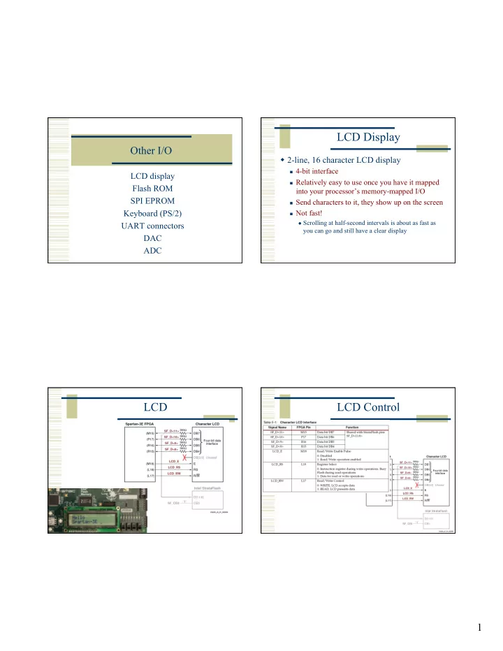
LCD Display
2-line, 16 character LCD display
4-bit interface Relatively easy to use once you have it mapped
into your processor’s memory-mapped I/O
Send characters to it, they show up on the screen Not fast! Scrolling at half-second intervals is about as fast as