32LG40 32LG40 32LG40 32LG40 Model : 32LG40 32 CLASS LCD HDTV w/ - - PowerPoint PPT Presentation

32lg40 32lg40 32lg40 32lg40
SMART_READER_LITE
LIVE PREVIEW

32LG40 32LG40 32LG40 32LG40 Model : 32LG40 32 CLASS LCD HDTV w/ - - PowerPoint PPT Presentation

TRAINING MANUAL TRAINING MANUAL TRAINING MANUAL TRAINING MANUAL 32LG40 32LG40 32LG40 32LG40 Model : 32LG40 32 CLASS LCD HDTV w/ BUILT-IN DVD PLAYER (31.5" diagonal) Direct View LCD Direct View LCD Direct View LCD Direct View


slide-1
SLIDE 1

32LG40 32LG40 32LG40 32LG40

Model : 32LG40 32” CLASS LCD HDTV w/ BUILT-IN DVD PLAYER (31.5" diagonal)

Direct View LCD Direct View LCD Direct View LCD Direct View LCD With built in DVD Player With built in DVD Player With built in DVD Player With built in DVD Player

TRAINING MANUAL TRAINING MANUAL TRAINING MANUAL TRAINING MANUAL

Original 08/12/2008 Updated 10/13/2010

slide-2
SLIDE 2

LCD DV August 2008 32LG40

2

OUTLINE OUTLINE OUTLINE OUTLINE

  • Main (Digital) Board
  • T-CON Board
  • Ballast Board

Circuit Board Operation, Troubleshooting of :

  • Switch mode Power Supply

Section 1 Section 2 Contact Information, Preliminary Matters, Specifications, LCD Overview, General Troubleshooting Steps, Signal Distribution, Disassembly Instructions and Voltages

slide-3
SLIDE 3

LCD DV August 2008 32LG40

3

32LG40 LCD Direct View Display

Section 1

This Section will cover Contact Information and remind the Technician of Important Safety Precautions for the Customers Safety as well as the Technician and the Equipment. Basic Troubleshooting Techniques which can save time and money sometimes can be overlooked. These techniques will also be presented. This Section will get the Technician familiar with the Disassembly, Identification and Layout of the LCD Display Panel. At the end of this Section the Technician should be able to Identify the Circuit Boards and have the ability and knowledge necessary to remove and replace safely any Circuit Board or Assembly.

Overview of Topics to be Discussed Overview of Topics to be Discussed Overview of Topics to be Discussed Overview of Topics to be Discussed

slide-4
SLIDE 4

LCD DV August 2008 32LG40

4

Important Safety Notice Important Safety Notice Important Safety Notice Important Safety Notice

The information in this training manual is intended for use by persons possessing an adequate background in electrical equipment, electronic devices, and mechanical systems. In any attempt to repair a major Product, personal injury and property damage can result. The manufacturer or seller maintains no liability for the interpretation of this information, nor can it assume any liability in conjunction with its use. When servicing this product, under no circumstances should the original design be modified or altered without permission from LG

  • Electronics. Unauthorized modifications will not only void the warranty, but may lead to property damage or

user injury. If wires, screws, clips, straps, nuts, or washers used to complete a ground path are removed for service, they must be returned to their original positions and properly fastened.

Caution Caution Caution Caution

To avoid personal injury, disconnect the power before servicing this product. If electrical power is required for diagnosis or test purposes, disconnect the power immediately after performing the necessary checks. Also be aware that many household products present a weight hazard. At least two people should be involved in the installation or servicing of such devices. Failure to consider the weight of an product could result in physical injury.

Preliminary Matters (The Fine Print) Preliminary Matters (The Fine Print) Preliminary Matters (The Fine Print) Preliminary Matters (The Fine Print)

slide-5
SLIDE 5

LCD DV August 2008 32LG40

5 Today’s sophisticated electronics are electrostatic discharge (ESD) sensitive. ESD can weaken or damage the electronics in a manner that renders them inoperative or reduces the time until their next failure. Connect an ESD wrist strap to a ground connection point or unpainted metal in the product. Alternatively, you can touch your finger repeatedly to a ground connection point or unpainted metal in the product. Before removing a replacement part from its package, touch the anti-static bag to a ground connection point or unpainted metal in the product. Handle the electronic control assembly by its edges only. When repackaging a failed electronic control assembly in an anti-static bag, observe these same precautions.

Regulatory Information Regulatory Information Regulatory Information Regulatory Information

This equipment has been tested and found to comply with the limits for a Class B digital device, pursuant to Part 15 of the FCC Rules. These limits are designed to provide reasonable protection against harmful interference when the equipment is operated in a residential installation. This equipment generates, uses, and can radiate radio frequency energy, and, if not installed and used in accordance with the instruction manual, may cause harmful interference to radio communications. However, there is no guarantee that interference will not occur in a particular installation. If this equipment does cause harmful interference to radio or television reception, which can be determined by turning the equipment off and on, the user is encouraged to try to correct the interference by one or more of the following measures: Reorient or relocate the receiving antenna; Increase the separation between the equipment and the receiver; Connect the equipment to an outlet on a different circuit than that to which the receiver is connected; or consult the dealer or an experienced radio/TV technician for help.

ESD Notice ESD Notice ESD Notice ESD Notice

(Electrostatic Static Discharge) (Electrostatic Static Discharge)

slide-6
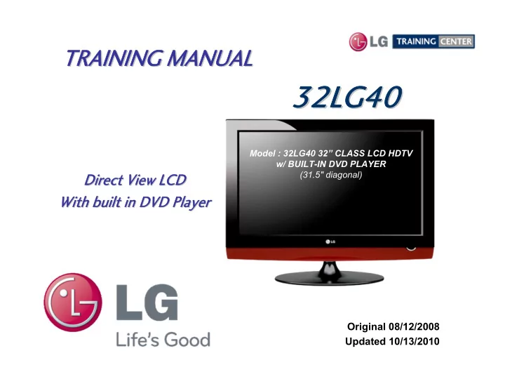
SLIDE 6

LCD DV August 2008 32LG40

6

Customer Service (and Part Sales) (800) 243-0000 Technical Support (and Part Sales) (800) 847-7597 USA Website (GSFS) http://gsfs-america.lge.com Customer Service Website http://www.us.lgservice.com Knowledgebase Website http://lgtechassist.com LG Web Training https://lge.webex.com LG CS Academy http://ln.lge.com/ilearn

Published August 2008 by LG Technical Support and Training LG Electronics Alabama, Inc. 201 James Record Road, Huntsville, AL, 35813. 32LG40, 32LH30, 37LH55, 42LG60, 42LG70, 42LH20, 42LH40, 42LH50, 42LH90, 42SL80, 47LG90, 47LH85, 42LE5500, 47LE8500 42PG20, 42PJ350, 42PQ20, 42PQ30, 50PG20, 50PJ350, 50PK250, 50PK750, 50PS80, 50PS60, 60PK750, 60PS11, 60PS60, 60PS80 LCD-DV: PLASMA: Also available on the Plasma Page: PDP Panel Alignment Handbook, Schematics with Bookmarks Plasma Control Board ROM Update (Jig required)

LG Contact Information LG Contact Information LG Contact Information LG Contact Information

Presentations with Audio/Video and Screen Marks

New Training Materials on New Training Materials on the Learning Academy site the Learning Academy site

New: 2010 Models Software Downloads Technical Assistance

http://136.166.4.200

slide-7
SLIDE 7

LCD DV August 2008 32LG40

7

Safety and Handling Regulations

1. Approximately 20 minute pre-run time is required before any adjustments are performed. 2. Refer to the Voltage Sticker on the Switch Mode Power Supply silk screening. (+/- ½ volt). 3. Be cautious of electric shock from the Backlight section, it uses high voltage AC. Check that the Power Supply and Drive Circuits are completely discharged because of residual current stored before Circuit Board removal. 4. C-MOS circuits are sensitive to static electricity. Use caution when dealing with these IC and circuits. 5. Exercise care when making voltage and waveform checks to prevent costly short circuits from damaging the unit. 6. Be cautious of lost screws and other metal objects to prevent a possible short in the circuitry. 1. Check the appearance of the Replacement Panel and Circuit Boards for both physical damage and part number accuracy. 2. Check the model label. Verify model names and board model matches. 3. Check details of defective condition and history. Example: Oscillator failure dead set, etc…

Checking Points to be Considered

OVERVIEW SECTION OVERVIEW SECTION OVERVIEW SECTION OVERVIEW SECTION

slide-8
SLIDE 8

LCD DV August 2008 32LG40

8

Basic Troubleshooting Steps Basic Troubleshooting Steps Basic Troubleshooting Steps Basic Troubleshooting Steps

Define, Localize, Isolate and Correct

  • Define

Look at the symptom carefully and determine what circuits could be causing the failure. Use your senses Sight, Smell, Touch and Hearing. Look for burned parts and check for possible overheated components. Capacitors will sometimes leak dielectric material and give off a distinct odor. Frequency of power supplies will change with the load, or listen for relay closing etc. Observation of the front Power LED may give some clues.

  • Localize

After carefully checking the symptom and determining the circuits to be checked and after giving a thorough examination using your senses the first check should always be the DC Supply Voltages to those circuits under test. Always confirm the supplies are not only the proper level but be sure they are noise free. If the supplies are missing check the resistance for possible short circuits.

  • Isolate

To further isolate the failure, check for the proper waveforms with the Oscilloscope to make a final determination of the failure. Look for correct Amplitude Phasing and Timing of the signals also check for the proper Duty Cycle of the signals. Sometimes “glitches” or “road bumps” will be an indication of an imminent failure.

  • Correct

The final step is to correct the problem. Be careful of ESD and make sure to check the DC Supplies for proper levels. Make all necessary adjustments and lastly always perform a Safety AC Leakage Test before returning the product back to the Customer.

slide-9
SLIDE 9

LCD DV August 2008 32LG40

9 This section of the manual will discuss the specifications of the 32LG40 “Thin” LCD Direct View Display Panel.

32LG40 Product Information 32LG40 Product Information 32LG40 Product Information 32LG40 Product Information

Side View

slide-10
SLIDE 10

LCD DV August 2008 32LG40

10

Basic Specifications Basic Specifications Basic Specifications Basic Specifications

  • 720p HD Resolution
  • 12,000:1 Dynamic Contrast Ratio
  • Side-loading Progressive Scan DVD Player
  • Super Multi-Format
  • 3x HDMI™ 1.3
  • AV Mode (Cinema, Sports, Game)
  • Clear Voice
  • SimpLink™ Connectivity
  • Invisible Speaker System
  • Expert Mode
  • PC Input
  • Swivel Stand (Manual)
slide-11
SLIDE 11

LCD DV August 2008 32LG40

11 HD RESOLUTION 720p HD Resolution Pixels: 1365 (H) × 768 (V) High definition television is the highest performance segment of the DTV system used in the US. It’s a wide screen, high-resolution video image, coupled with multi-channel, compact-disc quality sound.

Pixel Count to Resolution Comparisons Pixel Count to Resolution Comparisons Pixel Count to Resolution Comparisons Pixel Count to Resolution Comparisons FORMATS 480I 480P 1080I 720P 1080P Interlaced Progressive Interlaced Progressive Progressive Interlaced 2 Fields to make a Frame Progressive Each Field is a Frame Think of sync as the Panels “Refresh Rate” 240 Lines 480 Lines 540 Lines 720 Lines 1080 Lines NTSC SD HD HD HD Possible Frame Rates: 24FPS 30FPS 60FPS

768 720P Panel 720P Logo BASIC PIXEL COUNTS 720P Panel 1365 (H) × 768 (V) 1080P Panel 1920 (H) x 1080 (V)

slide-12
SLIDE 12

LCD DV August 2008 32LG40

12

Basic Specifications Basic Specifications Basic Specifications Basic Specifications

INVISIBLE SPEAKER SYSTEM LG’s 2008 line of TVs include a unique invisible speaker system, tuned by renowned audio expert, Mr. Mark Levinson. Speakers are embedded in strategic spots behind the front cabinet and use minute vibrations to turn the entire front bezel into the speaker system. The result is a clean, polished look, and enhanced audio by increasing the “sweet spot” giving a wider sound field. BUILT-IN SIDE LOADING PROGRESSIVE SCAN DVD PLAYER Save space with the built-in progressive scan DVD player. Side loading player upconverts DVDs to near 720p resolution and features LG “Super-Multi” technology which plays back almost any recordable disc based media. LG SIMPLINK™ MULTI-DEVICE CONTROL Allows for convenient control of other LG SimpLink products using the existing HDMI connection. HDMI (1.3 Deep Color) Digital multi-connectivity HDMI (1.3 Deep color) provides a wider bandwidth (340MHz, 10.2Gbps) than that of HDMI 1.2, delivering a broader range of colors, and also drastically improves the data-transmission speed.

slide-13
SLIDE 13

LCD DV August 2008 32LG40

13

Basic Specifications Basic Specifications Basic Specifications Basic Specifications

AV Mode "One click" - Cinema, Sports, Game mode. TAKE IT TO THE EDGE is a true multimedia TV with an AV Mode which allows you to choose from 3 different modes of Movies, Video Games and Sports by a single click of a remote control. Clear Voice Clearer dialogue sound Automatically enhances and amplifies the sound of the human voice frequency range to provide high-quality dialogue when background noise swells. Save Energy, Save Money Home electronic products use energy when they're off to power features like clock displays and remote controls. Those that have earned the ENERGY STAR use as much as 60% less energy to perform these functions, while providing the same performance at the same price as less-efficient models. Less energy means you pay less

  • n your energy bill. Draws less than 1 Watt in stand by.
slide-14
SLIDE 14

LCD DV August 2008 32LG40

14

Remote Control Remote Control Remote Control Remote Control

1 2 3 4 5 6 7 8 9

VOL CH FAV

MUTE

P A G E

LG TOP PORTION BOTTOM PORTION

p/n: MKJ40653818

slide-15
SLIDE 15

LCD DV August 2008 32LG40

15 Side Input Jacks

Rear and Side Input Jacks Rear and Side Input Jacks Rear and Side Input Jacks Rear and Side Input Jacks

USB HDMI Composite A/V Main Board Orientation Component Y Pr/Pb Optical Audio RGB (PC) Audio RGB (PC) HDMI RS232 Service Only Remote In Audio Out Composite

Current Software Release 32LG40-UA-v03.12_080711_Download.epk

slide-16
SLIDE 16

LCD DV August 2008 32LG40

16

Accessing the Service Menu Accessing the Service Menu Accessing the Service Menu Accessing the Service Menu

REMOTE TOP PORTION SIDE KEYS

Note: Dependant upon the Software Version, a Password may be required to enter the Service Menu. If a password is required, enter 0000 To access the Service Menu. 1) Turn the Set On 2) Simultaneously, Press and “Hold” the Menu Key on the Side Key pad and Press and “Hold” the Menu Key on the Remote approximately 5 seconds. 3) If Customer’s Menu appears, continue to hold until it disappears. 4) The Service Menu appears

slide-17
SLIDE 17

LCD DV August 2008 32LG40

17 1) Create an LG_DTV folder on the USB Flash Drive 2) Copy new software (xxx.epk) to "LG_DTV"

  • folder. Make sure to have correct software file.

3) With TV turned on, insert USB flash drive. 4) You can see the message “TV Software Upgrade” (See figure to right) 5) Cursor left and highlight "START" Button and push “Enter” button using the remote control. 6) You can see the download progress Bar. 7) Do not unplug until unit has automatically restarted. 8) When download is completed, you will see “COMPLETE”. 9) Your TV will be restarted automatically.

Software Upgrade Procedure Software Upgrade Procedure Software Upgrade Procedure Software Upgrade Procedure

Shows the Currently Installed Version Shows the Software Version found on the USB Flash Drive Shows the Software file found

  • n the USB Flash

Drive

* CAUTION: Do not remove AC power or the USB Flash Drive. Do not turn off Power, during the upgrade process.

slide-18
SLIDE 18

LCD DV August 2008 32LG40

18

32LG40 Product Measurements 32LG40 Product Measurements 32LG40 Product Measurements 32LG40 Product Measurements

slide-19
SLIDE 19

LCD DV August 2008 32LG40

19

This section of the manual will discuss troubleshooting. Upon completion of this section the Technician will have a better understanding of how to diagnosis and resolve problems.

TROUBLESHOOTING SECTION TROUBLESHOOTING SECTION TROUBLESHOOTING SECTION TROUBLESHOOTING SECTION

slide-20
SLIDE 20

LCD DV August 2008 32LG40

20

Removing the Back Cover Removing the Back Cover Removing the Back Cover Removing the Back Cover

The Stand does not need to be removed. Remove the 18 screws shown by arrows. Pay attention to the size and type of screw as there are many different types. Putting in the improper screw when reassembling may Cause damage.

slide-21
SLIDE 21

LCD DV August 2008 32LG40

21

Circuit Board Layout Circuit Board Layout Circuit Board Layout Circuit Board Layout

Panel p/n EAJ41825601

Side Inputs Side Controls LVDS Cables Speakers Speaker rattle. 1) Tighten screws at bottom of cabinet 2) Tighten screws holding woofers

T-CON p/n EAT56801301 Ballast p/n EAY56797501

slide-22
SLIDE 22

LCD DV August 2008 32LG40

22

Invisible Speaker System Layout Invisible Speaker System Layout Invisible Speaker System Layout Invisible Speaker System Layout

Bottom View of Woofer Ports

Woofers Tweeters Tweeters

Stand Removed Speaker rattle. 1) Tighten screws at bottom of cabinet 2) Tighten screws holding woofers

slide-23
SLIDE 23

LCD DV August 2008 32LG40

23

POWER SUPPLY POWER SUPPLY POWER SUPPLY POWER SUPPLY SECTION SECTION SECTION SECTION

P201 AC IN P203

To Main

F100 5A/250V AC IN

To Ballast 1 2 Error WM-D1 INV On/Off BR1 Gnd Gnd Gnd Gnd Gnd 24V 24V 24V 24V 24V 14 13 12 11 10 9 8 7 6 5 4 3 2 1

n/c F101 3.15A/250V 334V Actual

1

Hot Ground

n/c PWR-DIM INVOn/Off ACD Gnd Gnd 5.2V 5.2V Gnd 12V Gnd 16.5V 24 22 20 18 16 14 12 10 8 6 4 2 Fixed Volts BR1 POWER-ON ERROR Gnd Gnd 5.2V 5.2V Gnd 12V Gnd 16.5V 23 21 19 17 15 13 11 9 7 5 3 1

SMPS Board Layout SMPS Board Layout SMPS Board Layout SMPS Board Layout

slide-24
SLIDE 24

LCD DV August 2008 32LG40

24

Power Supply (SMPS) Power Supply (SMPS) Power Supply (SMPS) Power Supply (SMPS) Board Drawing Board Drawing Board Drawing Board Drawing

P201 AC IN P203

To Main

F100 5A/250V AC IN

To Ballast 16.5V Gnd 12V Gnd 5.2V 5.2V Gnd Gnd ACD INVOn/Off PWR-DIM n/c 2 4 6 8 10 12 14 16 18 20 22 24 16.5V Gnd 12V Gnd 5.2V 5.2V Gnd Gnd ERROR POWER-ON BR1 fixedV 1 3 5 7 9 11 13 15 17 19 21 23 Error WM-D1 INV On/Off BR1 Gnd Gnd Gnd Gnd Gnd 24V 24V 24V 24V 24V 14 13 12 11 10 9 8 7 6 5 4 3 2 1

F101 3.15A/250V 334V Actual

slide-25
SLIDE 25

LCD DV August 2008 32LG40

25

Power Supply P201 Control Si Power Supply P201 Control Signals from Main Board P800 gnals from Main Board P800 Power Supply P201 Control Si Power Supply P201 Control Signals from Main Board P800 gnals from Main Board P800

slide-26
SLIDE 26

LCD DV August 2008 32LG40

26

Power Supply Board Test (1) All Board Disconnected Power Supply Board Test (1) All Board Disconnected Power Supply Board Test (1) All Board Disconnected Power Supply Board Test (1) All Board Disconnected

The Power Supply “MUST” be producing STAND-BY +5V before proceeding. P201 Connector disconnected from the Main Board AC: Not applied when adding jumper. Applied when making test.

With Power Supply disconnected from other Boards and AC applied, confirm that the Power Supply is producing 5V from either Pins 9, 10, 11 or 12. If not, check fuse. If fuse OK and no 5V, replace Power Supply. If 5V OK then continue. 1st short either pin 9, 10, 11 or 12 (5V) to Pin 19 (PWR) using a 10K resistor. This turns on the power supply. Confirm that the other low voltage power supplies are activated. Pins 1 and 2 (16V) Pins 5 and 6 (12V) Pin 18 (AC Detect) goes high Fuse F101 Check for 350V (Ballast Voltage) If any voltage missing, replace Power Supply.

+5V

slide-27
SLIDE 27

LCD DV August 2008 32LG40

27

Power Supply Board Test (2) Checking the Backlights Power Supply Board Test (2) Checking the Backlights Power Supply Board Test (2) Checking the Backlights Power Supply Board Test (2) Checking the Backlights

If the 1st test was successful, continue. Leave original 10K in place. 2nd: To test the Backlights, leave the 10K jumper in place. Plug up the Back light plug P203. Apply AC Power. Observe the Backlights. If normal, LED1 on the Ballast Board should turn on first, then backlights should turn on and LED1 should go off.. If no backlight activity, confirm the Fuse F101 has approx. 350V on both sides. If on one side, check fuse for open. If no 350V, replace Power Supply. If 300V present, check P203 for 24V on Pins 1~5. Check P203 Pin 12 for at least 3V (Inverter On/Off). If yes, confirm Connectors to backlight OK, if OK, then panel defective.

+5V P2 Connector disconnected from the Main Board AC: Not applied when adding jumper. Applied when make test. Ballast will not run if either of the Backlight plugs are removed.

slide-28
SLIDE 28

LCD DV August 2008 32LG40

28

Power Supply Board Removal Power Supply Board Removal Power Supply Board Removal Power Supply Board Removal

Disconnect P203, P201 and AC In Remove the 4 screws indicated in the red circles.

slide-29
SLIDE 29

LCD DV August 2008 32LG40

29

Power Supply Connector P201 Odd Power Supply Connector P201 Odd Pins Voltage and Diode Check Pins Voltage and Diode Check Power Supply Connector P201 Odd Power Supply Connector P201 Odd Pins Voltage and Diode Check Pins Voltage and Diode Check

Resistance taken in Diode Mode with Connectors Removed 0.31V 16V 0V 16.5V 1 Gnd Gnd Gnd Gnd 3 1.69V 11.8V 0V 12V 5 Gnd Gnd Gnd Gnd 7 0.34V 5.15V 5.15V 5.2V 9 0.34V 5.15V 5.15V 5.2V 11 Gnd Gnd Gnd Gnd 13 Gnd Gnd Gnd Gnd 15 1.26V Gnd Gnd ERR 17 OL 2.86V 0V PWR 19 OL 1.68V 0V BR1 21 OL 3.2V 0V N/C 23 Diode Check Run STBY Label Pin

P201 "SMPS" to P800 "Main Board"

Gnd Gnd Gnd Gnd 4 0.31V 16V 0V 16.5V 2 1.69V 11.8V 0V 12V 6 0V Gnd Gnd Gnd 8 0.34V 5.15V 5.15V 5.2V 10 0.34V 5.15V 5.15V 5.2V 12 Gnd Gnd Gnd Gnd 14 Gnd Gnd Gnd Gnd 16 OL 4.57V 5.05V ACD 18 OL 3.29V 0V INV On/Off 20 OL 3.38V 0V PWM-DIM 22 OL 0V 0V N/C 24 Diode Check Run STBY Label Pin

slide-30
SLIDE 30

LCD DV August 2008 32LG40

30

Power Supply Connector P203 Voltage and Diode Check Power Supply Connector P203 Voltage and Diode Check Power Supply Connector P203 Voltage and Diode Check Power Supply Connector P203 Voltage and Diode Check

Resistance taken in Diode Mode with Connectors Removed OL 0V 0V ERROR 14 OL 3.40V 0V PWM-DIM 13 OL 3.45V 0V INV On-Off 12 OL 1.67V 0V BR1 11 Gnd Gnd Gnd Gnd 10 Gnd Gnd Gnd Gnd 9 Gnd Gnd Gnd Gnd 8 Gnd Gnd Gnd Gnd 7 Gnd Gnd Gnd Gnd 6 0.33V 24.52V 0V 24V 5 0.33V 24.52V 0V 24V 4 0.33V 24.52V 0V 24V 3 0.33V 24.52V 0V 24V 2 0.33V 24.52V 0V 24V 1 Diode Check Run STBY Label Pin

P203 "SMPS" to MCN1 "Ballast Board"

slide-31
SLIDE 31

LCD DV August 2008 32LG40

31

MAIN BOARD SECTION MAIN BOARD SECTION MAIN BOARD SECTION MAIN BOARD SECTION

P800 P901 P900 P904 P401 P500 P902 P200 No Connection Software Download LVDS To T-CON To Power To DVD To DVD To DVD To Ft Keys To SPK

Reset BCM IC407 Micro

Side Inputs HDMI USB

TUNER

LD800

IC100 BCM

IC101 Flash Memory BCM IC803 9V Reg IC809 A2.6V BCM Reg IC807 5V Reg IC806 A3.3V BCM IC802 3.3V Reg IC600 HDMI Selector IC800 CVBS Amp IC304 DDR VTT IC301 IC303 IC300 IC302 IC400 BCM Reset Q801 5V Sub Switch IC501 Audio Processor and Output 16V Pins 49~52 IC602 HDMI EDID IC502 Audio Selector IC402 Serial Port Interface IC201 USB 3.3V X400 24Mhz Q800 SIF IC601 HDMI EDID X200 54Mhz Dual Data Registers IC405 Micro Reset Q400 Micro Reset Q802 5V Sub Switch Control

If odd Video problems are found, use some freeze spray about IC100 and its circuits, If video returns to normal, Board needs to be replaced.

slide-32
SLIDE 32

LCD DV August 2008 32LG40

32

Main Board (Front Side) Regulator Checks 1 of 2 Main Board (Front Side) Regulator Checks 1 of 2 Main Board (Front Side) Regulator Checks 1 of 2 Main Board (Front Side) Regulator Checks 1 of 2

3.39V 0V Reset (Lo-Hi) OUT 3 9V 0V +9V OUT 3 Gnd Gnd Gnd Gnd 2 Gnd Gnd Gnd Gnd 2 3.4V 0V D3.3V_BCM IN 1 12V 0V +12V IN 1 RUN STBY NAME FUNCTION PIN RUN STBY NAME FUNCTION PIN RESET GENERATOR TO IC401 3.3BCM (On Back) IC400 +9V Regulator IC803 1.29V 0V DDRO_VTT On/Off Control 4 3.2V 0V +5V_SUB IN 3 2.6V 0V D2.6V_BCM IN 5,6,7 Gnd Gnd Gnd OUT 2 1.29V 0V DDRO_VTT OUT 3,8 5V 0V +3.3V Gnd 1 RUN STBY NAME FUNCTION PIN RUN STBY NAME FUNCTION PIN 2.6V BCM IC304 +3.3V Regulator (3.3V TMDS_SW) IC802 3.1V 0V +3.3V OUT 8 0.6V 0.6V Reset (Lo-Hi) OUT 3 5V 0V USB_PWR_Out_1 OUT 7 Gnd Gnd Gnd Gnd 2 3.4V 0V BCM DDR Power On/Off Control 3 3.41V 3.41V 3.3V_MICON IN 1 5V 0V +5V IN 2 RUN STBY NAME FUNCTION PIN RUN STBY NAME FUNCTION PIN RESET GENERATOR FOR Q400 Micro Reset IC405 USB Power IC201

slide-33
SLIDE 33

LCD DV August 2008 32LG40

33

Main Board (Front Side) Regulator Checks 2 of 2 Main Board (Front Side) Regulator Checks 2 of 2 Main Board (Front Side) Regulator Checks 2 of 2 Main Board (Front Side) Regulator Checks 2 of 2

Gnd Gnd Gnd Gnd 11,18,19,20 n/c n/c n/c n/c 14,15 2.66V 0V D2.6V_BCM OUT 1,2,3,4,5 3.41V 0V Power_CTL_2.6V On/Off Control 17 4.98V 0.36V +5V_SUB IN 6,7,8,10 Gnd Gnd Gnd Gnd E RUN STBY NAME FUNCTION PIN 0V 0V 3.3VVST_MICON Vcc C D2.6V/A2.6V_BCM Regulator IC809 0.6V 0.6V Reset Reset B Gnd Gnd Gnd Gnd 5 RUN STBY NAME FUNCTION PIN n/c n/c n/c n/c 4 RESET GENERATOR FOR MICRO IC407 Q400 5V 0V +5V OUT 3 Gnd Gnd Gnd Gnd E 3.4V 0V Power_CTL_3.3V On/Off Control 2 5V 0V ST_5V Pull Down C 8.9V 0V +9V IN 1 3.29V 0V RL_ON On/Off Control B RUN STBY NAME FUNCTION PIN RUN STBY NAME FUNCTION PIN D3.3V/A3.3V_BCM Regulator IC807 CONTROLLER for 5V SUB SWITCH Q801 Q802 3.4V 0.1V D3.3V_BCM OUT 4 5V 0V +5V_SUB OUT 5,6,7,8 Gnd Gnd Gnd Gnd 3 0.28V 0V Q802 On/Off Control 2,4 5V 0.36V +5V_SUB IN 2 5V 0V ST_5V IN 1,3 3.4V 0V Power_CTL_3.3V On/Off Control 1 RUN STBY NAME FUNCTION PIN RUN STBY NAME FUNCTION PIN 5V SUB SWITCH Q801 D3.3V/A3.3V_BCM Regulator turns on LD800 IC806

slide-34
SLIDE 34

LCD DV August 2008 32LG40

34

Main Board (Back View) Regulator Layout Main Board (Back View) Regulator Layout Main Board (Back View) Regulator Layout Main Board (Back View) Regulator Layout

TUNER TU800

P800 P901 P900 P904 P401 P500 P902 P200

IC808 3.3V Micon 1 16 IC102 HDCP KEY IC403 NVRAM IC805 A1.2V BCM Reg IC702 EEPROM Q901 LVDS 12V Switch Q900 Turns on Q901 IC406 Micro EEPROM X200

Side Inputs

IC408 SIF Select DVD/BCM IC701 Side HDMI EDID IC801 1.8V Reg IC401 BCM Reset Silk Screen for Pin 1 wrong IC805

slide-35
SLIDE 35

LCD DV August 2008 32LG40

35

Main Board (Back Side) Regulator Checks Main Board (Back Side) Regulator Checks Main Board (Back Side) Regulator Checks Main Board (Back Side) Regulator Checks

Screen Print for Pin No is incorrect, use IC Gnd Gnd Gnd Gnd 11,12,18, 19,20 0V 0V n/c n/c 13, 14,15,16 12.36V 0V LVDS 12V OUT 5,6,7,8 1.29V 0V D1.2V_BCM OUT 1,2,3,4,5 6.16V 0V Q900 On/Off Control 2,4 3.41V 0V Power_CTL_1.2V On/Off Control 17 12.36V 0V 12V IN 1,3 5V 0.38V +5V_SUB IN 6,7,8,10 RUN STBY NAME FUNCTION PIN RUN STBY NAME FUNCTION PIN LVDS 12V SWITCH Q901 D1.2V/A1.2V BCM REGULATOR IC805 0V 0V Gnd Gnd E 3.29V 0.26V 3.3V_TMDS_SW IN 3 0V 0V LVDS Switch Control Pull Down 12V C 1.8V 0V '+1.8V_NTP OUT 2 0.75V 0V LVDS_PANEL_CTRL Control B Gnd Gnd Gnd Gnd 1 RUN STBY NAME FUNCTION PIN RUN STBY NAME FUNCTION PIN LVDS 12V SWITCH CONTROLLER Q901 Q900 +1.8V_NTP REGULATOR IC801 Gnd Gnd Gnd Gnd 4 3.4V 0V BCM_RESET OUT 6 3.43V 3.43V 3.3VST_MICON OUT 3 3.4V 0V Reset from IC400 On/Off Control 1 5V 5V ST_5V IN 2 3.41V 0V D3.3V_BCM IN 14 RUN STBY NAME FUNCTION PIN RUN STBY NAME FUNCTION PIN ST-BY 3.3V DC-DC CONVERTER IC808 BCM RESET IC401

slide-36
SLIDE 36

LCD DV August 2008 32LG40

36 2.4Vp/p 24Mhz With set on or off

X400

Main Board X400 and X200 Check Main Board X400 and X200 Check Main Board X400 and X200 Check Main Board X400 and X200 Check

Main Board X400 Location Main Board X200 Location MAIN Board 660mVp/p 54Mhz Only when set is on

X200

1.49V 1.49V 1.49V 1.49V TP Use Crystal Side R232 or R233 TP Use Crystal leg top or bottom IC407 Micro

slide-37
SLIDE 37

LCD DV August 2008 32LG40

37

Main Board Tuner Video and SI Main Board Tuner Video and SIF Output Check Pin Location F Output Check Pin Location Main Board Tuner Video and SI Main Board Tuner Video and SIF Output Check Pin Location F Output Check Pin Location

For Easy Access, pop the shield off the tuner If you leave the shield on you can still access the same pins. Be careful not to accidentally ground out your test lead on the shield.

Pin 16 Composite Video Pin 14 Audio SIF Pin 3 Tuner B+ (5V)

slide-38
SLIDE 38

LCD DV August 2008 32LG40

38 MAIN Board

Main Board Tuner Video and SIF Output Check Main Board Tuner Video and SIF Output Check Main Board Tuner Video and SIF Output Check Main Board Tuner Video and SIF Output Check

Tuner Location 1Vp/p 20uSec rate Pin 16 “Video” Signal Pin 14 “SIF” Signal 850mVp/p Using SMTP Color Bar Input Using SMTP Color Bar Input

slide-39
SLIDE 39

LCD DV August 2008 32LG40

39

Main Board LVDS P902 Output Check Main Board LVDS P902 Output Check Main Board LVDS P902 Output Check Main Board LVDS P902 Output Check

P902 Location To confirm that the Main Board is outputting Picture Content signals, check P902 (LVDS) cable for

  • utput. Check 11~20. This signals vary from each other, but looking for signals like the ones

shown below on any of these pins confirm the output of video content. This signal is using standard SMTE Color Bar output from a generator as the input source. Pin 11 Pin 16 MAIN Board Remember there are actually 10 pins with LVDS signals. This only represents two Waveforms as an example.

slide-40
SLIDE 40

LCD DV August 2008 32LG40

40

Main Board Removal Main Board Removal Main Board Removal Main Board Removal

Disconnect P902, P800, P901, P900, P904, P401 and P500 Note: In the top right is a Connector P200. This is an open

  • connection. (Software Upgrades)

Remove the 2 screws securing the Side input decorative plastic piece on the right. Remove the 4 screws securing the Main Board indicated below in red. Remove the Right side decorative plastic piece by removing top and bottom screws. Remove the remaining 6 screws that remove the “Shield” covering the Main Board. Careful at this point, the Board will Swing free of the supports.

slide-41
SLIDE 41

LCD DV August 2008 32LG40

41

Main Board Connector P800 Voltage and Diode Check Main Board Connector P800 Voltage and Diode Check Main Board Connector P800 Voltage and Diode Check Main Board Connector P800 Voltage and Diode Check

Resistance taken in Diode Mode with Connectors Removed OL 0V 0V n/c 24 OL 3.2V 0V n/c 23 2.15V 3.38V 0V VBR-B 22 OL 1.68V 0V BR1 21 2.15V 3.29V 0V INV-On/Off 20 1.25V 2.86V 0V RL-ON 19 OL 4.57V 5V AC-DET 18 OL 3.3V 0V VBR-B 5V-MNT 17 Gnd Gnd Gnd Gnd 15, 16 Gnd Gnd Gnd Gnd 13, 14 1.23V 5.15V 5V ST-5V 11, 12 1.23V 5.15V 5V ST-5V 9, 10 Gnd Gnd Gnd Gnd 7, 8 3.03V 11.8V 0V 12V 5, 6 Gnd Gnd Gnd Gnd 3, 4 OL 16V 0V 16V 1, 2 Diode Check Run STBY Label Pin

P800 Connector "Main" to P201 "SMPS Board"

slide-42
SLIDE 42

LCD DV August 2008 32LG40

42

Main Board Connector P902 LVDS Layout and 12V Circuit Main Board Connector P902 LVDS Layout and 12V Circuit Main Board Connector P902 LVDS Layout and 12V Circuit Main Board Connector P902 LVDS Layout and 12V Circuit

LVDS Signal Waveforms Shown on back of Interconnect Diagram Panel Control from IC407 Pin 33 Q900 turns on Q901 LVDS Switch generating LVDS 12V All voltages are shown on the Interconnect Diagram

LVDS 12V

For Locations See Main Board Back Side View

slide-43
SLIDE 43

LCD DV August 2008 32LG40

43

Main Board Connector P902 Even Main Board Connector P902 Even Pins Voltage and Diode Check Pins Voltage and Diode Check Main Board Connector P902 Even Main Board Connector P902 Even Pins Voltage and Diode Check Pins Voltage and Diode Check

Resistance taken in Diode Mode with Connectors Removed 3V 3.07V 0.4V Size Sel 25 Gnd n/c 0V n/c 23 OL n/c 0V n/c 21 1.11V 1.14V 0V LVDS 19 1.11V 1.08V 0V LVDS 17 1.06V 1.1V 0V LVDS 15 1.11V 1.2V 0V LVDS 13 0.98V 1.2V 0V LVDS 11 Gnd 0V 0V Gnd 9 Gnd 0V 0V Gnd 7 Gnd 0V 0V Gnd 5 OL 12.3V 0V LVDS 12V 3 OL 12.3V 0V LVDS 12V 1 Diode Check Run SBY Label Pin Gnd 0V 0V Gnd 26 OL n/c 0V n/c 24 OL n/c 0V n/c 22 1.06V 1.06V 0V LVDS 20 1.06V 1.13V 0V LVDS 18 1.05V 1.09V 0V LVDS 16 1.06V 1.05V 0V LVDS 14 0.98V 1.1V 0V LVDS 12 Gnd 0V 0V Gnd 10 Gnd 0V 0V Gnd 8 Gnd 0V 0V Gnd 6 OL 12.3V 0V LVDS 12V 4 OL 12.3V 0V LVDS 12V 2 Diode Check Run SBY Label Pin

P902 Connector "Main" to CN1 “T-CON Board"

slide-44
SLIDE 44

LCD DV August 2008 32LG40

44

Main Board Connector P401 Voltage and Diode Check Main Board Connector P401 Voltage and Diode Check Main Board Connector P401 Voltage and Diode Check Main Board Connector P401 Voltage and Diode Check

Resistance taken in Diode Mode with Connectors Removed Gnd 0V 0V Gnd 15 0.8V 0V 2.1V LED-R 14 0.8V 2.1V 0V LED-G 13 Gnd 0V 0V Gnd 12 OL 0V 0V n/c 11 2.3V 4.1V 4.1V IR 10 0.8V 0V 0V PWM-LED 9 0.53V 5V 5V ST-5V 8 OL 0V 0V n/c 7 1.4V 3.4V 3.4V KEY-2 6 1.4V 3.4V 3.4V KEY-1 5 Gnd 0V 0V Gnd 4 Gnd 0V 0V Gnd 3 1.4V 3.4V 3.4V KEY4 2 1.4V 3.4V 3.4V KEY3 1 Diode Check Run STBY Label Pin

P401 Connector "Main Board" to "Front Keys"

slide-45
SLIDE 45

LCD DV August 2008 32LG40

45

Main Board Connector P904 Voltage and Diode Check Main Board Connector P904 Voltage and Diode Check Main Board Connector P904 Voltage and Diode Check Main Board Connector P904 Voltage and Diode Check

Resistance taken in Diode Mode with Connectors Removed Gnd 0V 0V Gnd 13 0.83V 0V 0V n/c 12 Gnd 0V 0V Gnd 11 OL 0V 0V n/c 10 Gnd 0V 0V Gnd 9 OL 0.6V 0V Y 8 OL 0.8V 0V Pb 7 OL 0.8V 0V Pr 6 Gnd Gnd 0V Gnd 5 OL 3.3V 3.34V n/c 4 OL 3.3V 3.34V n/c 3 1.60V * 3.3V *3.3V Disc Chedk 2 OL 3.34V 3.34V n/c 1 Diode Check Run SBY Label Pin OL 0V 0V n/c 26 Gnd 0V 0V Gnd 25 OL 0V 0V n/c 24 OL 0V 0V n/c 23 Gnd 0V 0V Gnd 22 OL 0V 0V n/c 21 OL 2.4V 0V DVD-R-In2 20 Gnd 0V 0V Gnd 19 OL 2.4V 0V DVD-L-In2 18 OL 0V 0V DVD-MUTE 17 0.83V 1.8V 3.38V DVD-SPDIF 16 OL 0V 0V n/c 15 OL 0.7V 0V n/c 14 Diode Check Run SBY Label Pin

P904 Connector "Main" to CN401 "DVD Player"

*Pin 2: 3.3V With Disc Player and 0V No Disc Player

slide-46
SLIDE 46

LCD DV August 2008 32LG40

46

Main Board Connectors P900, P901 Main Board Connectors P900, P901, P500 and , P500 and P200 Voltage and Diod P200 Voltage and Diod Main Board Connectors P900, P901 Main Board Connectors P900, P901, P500 and , P500 and P200 Voltage and Diod P200 Voltage and Diode Check e Check e Check e Check

Resistance taken in Diode Mode with Connectors Removed Gnd 0V Gnd Gnd 4 3V 3.4V 0.7V DVDP-TXD 3 3V 3.08V 0.7V DVDP-RXD 2 1.68V *3.4V *3.4V Disk-Enable 1 Diode Check Run SBY Label Pin P900 Connector "Main" to P402 "DVD Player" 0.45V 5.01 0V 5V 6 Gnd 0V 0V Gnd 5 Gnd 0V 0V Gnd 4 .099V 3.37V 3.4V DVDP 3.3V 3 Gnd 0V 0V Gnd 2 3V 12.3V 0V 12V 1 Diode Check Run SBY Label Pin P901 Connector "Main" to CN400 "DVD Player" 2.78V 8.15V 0V L- 4 2.78V 8.15V 0V L+ 3 2.78V 8.14V 0V R- 2 2.78V 8.14V 0V R+ 1 Diode Check Run SBY Label Pin P500 Connector "Main" to "Speakers" Gnd 0V 0V Gnd 4 OL 5V 0V SDA 3 OL 5V 0V SCL 2 OL 5V 0V Vcc 1 Diode Check Run SBY Label Pin P200 Connector "Main" Software Download *Pin 1: 3.4V with No Disc and 0V with Disc inserted

slide-47
SLIDE 47

LCD DV August 2008 32LG40

47

MCN1 To Backlight Right Side To Backlight Left Side Transformers Ballast Start Det LED (LED1) F1 8A/125V

p/n EAY56797501

BALLAST SECTION (With Shield) LAYOUT BALLAST SECTION (With Shield) LAYOUT BALLAST SECTION (With Shield) LAYOUT BALLAST SECTION (With Shield) LAYOUT

slide-48
SLIDE 48

LCD DV August 2008 32LG40

48

Ballast Board Assembly Layout Ballast Board Assembly Layout Ballast Board Assembly Layout Ballast Board Assembly Layout

MCN1 Ballast Start Det LED LED1 To Backlight Right Side To Backlight Left Side Transformers F1 8A/125V

slide-49
SLIDE 49

LCD DV August 2008 32LG40

49

Ballast Transformer Waveforms Ballast Transformer Waveforms Ballast Transformer Waveforms Ballast Transformer Waveforms

T1/T2 Pin 6 Transformers

  • T1/T2 Pin 1

34V p/p 64.89kHz 22.2V p/p 220kHz Primary Side Warning, secondary is

  • ver 1.2Kv
slide-50
SLIDE 50

LCD DV August 2008 32LG40

50

Ballast Control Signals Ballast Control Signals from Main Board P800 from Main Board P800 Ballast Control Signals Ballast Control Signals from Main Board P800 from Main Board P800

slide-51
SLIDE 51

LCD DV August 2008 32LG40

51

Backlight Drive Backlight Drive Backlight Drive Backlight Drive Signal Effects Signal Effects Signal Effects Signal Effects

PWMDIM manipulates the Burst Triangle Oscillator in the ballast drive IC. ADIM also manipulates the Burst Triangle Oscillator But it is not used. Waveform Just for Explanation, taken from a different chassis.

slide-52
SLIDE 52

LCD DV August 2008 32LG40

52

Ballast Removal (Heat Sink and Insu Ballast Removal (Heat Sink and Insulators) lators) Ballast Removal (Heat Sink and Insu Ballast Removal (Heat Sink and Insulators) lators)

Protects the Outputs Insulator Insulator Shiny Side Down (Conductive) Be sure to replace “All” heat sink materials and insulators. Cut Out Alignment Notch Alignment Notch Heat Transfer Material S h i e l d

p/n EAY56797501

slide-53
SLIDE 53

LCD DV August 2008 32LG40

53

Ballast Connector MCN1 Vo Ballast Connector MCN1 Voltage and Diode Check ltage and Diode Check Ballast Connector MCN1 Vo Ballast Connector MCN1 Voltage and Diode Check ltage and Diode Check

Resistance taken in Diode Mode with Connectors Removed Gnd Gnd Gnd Gnd_2 14 OL 3.40V 0V VBR_B 13 OL 3.45V 0V On/Off 12 OL 1.67V 0V BVR_A 11 Gnd Gnd Gnd Gnd_1 10 Gnd Gnd Gnd Gnd 9 Gnd Gnd Gnd Gnd 8 Gnd Gnd Gnd Gnd 7 Gnd Gnd Gnd Gnd 6 OL 24.52V 0V VBL 5 OL 24.52V 0V VBL 4 OL 24.52V 0V VBL 3 OL 24.52V 0V VBL 2 OL 24.52V 0V VBL 1 Diode Check Run STBY Label Pin MCN1 "Ballast" to P203 "SMPS"

slide-54
SLIDE 54

LCD DV August 2008 32LG40

54

T T-

  • CON (TFT DRIVE) SECTION

CON (TFT DRIVE) SECTION CON (TFT DRIVE) SECTION CON (TFT DRIVE) SECTION

CN1 LVDS To Main Remove Screw Remove Screw Remove One Screw at the to of the Brace then Remove LVDS and three screws. Remove Screw

T T-

  • CON

CON (TFT DRIVE) Board Removal) (TFT DRIVE) Board Removal) CON CON (TFT DRIVE) Board Removal) (TFT DRIVE) Board Removal)

slide-55
SLIDE 55

LCD DV August 2008 32LG40

55

T T-

  • CON (TFT Drive) Board Layout

CON (TFT Drive) Board Layout CON (TFT Drive) Board Layout CON (TFT Drive) Board Layout

CN2 CN3 CN1 LVDS US2 To Main To TFT Panel To TFT Panel Use the Connector P902 on Main Board for Voltages and Signal Readings

3) 0.0V 2) 1.8V 1) 3.3V

US2

12V F1 6.3V/1.5A

Remember to put the three screws back in for ground purposes.

p/n EAT56801301

slide-56
SLIDE 56

LCD DV August 2008 32LG40

56

T T-

  • CON (TFT Drive) Board DC to DC Converter Voltages for Panel

CON (TFT Drive) Board DC to DC Converter Voltages for Panel CON (TFT Drive) Board DC to DC Converter Voltages for Panel CON (TFT Drive) Board DC to DC Converter Voltages for Panel

The voltages developed by US1 are used on the T-CON and for the X and Y drivers inside the TFT panel. * The Voltages on CN2 and CN3 must be present for the panel to operate.

US1 Voltages

6.6V 48 3.3V 32 0V 16 0V 47 .6V 31 0V 15 6.6V 46 1.8V 30 6.9V 14 6.6V 45 4.3V 29 15.0V 13 6.6V 44 V0V 28 4.8V 12 15.0V 43 12.0V 27 0V 11 15.0V 42 12.0V 26 1.2V 10 1.2V 41 12.0V 25 21.0V 9 0V 40 3.3V 24 19.70 8 15.0V 39 3.3V 23 5.4V 7 12.0V 38 11.3V 22 3.3V 6 12.0V 37 1.2V 21 1.9V 5 0V 36 0V 20 0.7V 4 0V 35 0V 19 2.4V 3 0V 34 4.3V 18 6.6V 2 6.0V 33 1.2V 17 6.6V 1 DC Pin DC Pin DC Pin US1 Voltages

slide-57
SLIDE 57

LCD DV August 2008 32LG40

57

T T-

  • CON Board Removal (LVDS Removal)

CON Board Removal (LVDS Removal) CON Board Removal (LVDS Removal) CON Board Removal (LVDS Removal)

Disconnect CN1 LVDS Cable CAUTION: When removing LVDS Cables, be careful. Press the release Tabs to avoid damage to Board or to the Cable itself.

LVDS Connectors Press in from the sides and lift out. Press in Press in

slide-58
SLIDE 58

LCD DV August 2008 32LG40

58

T T-

  • CON Board Connector CN1Vo

CON Board Connector CN1Voltage an ltage and Diode Check d Diode Check CON Board Connector CN1Vo CON Board Connector CN1Voltage an ltage and Diode Check d Diode Check

Resistance taken in Diode Mode with Connectors Removed

CN1 Connector "T-CON" Odd to P902 "Main"

Gnd 0V 0V Gnd 26 OL 3.07V 0.4V Size Sel 25 n/c n/c 0V n/c 24 n/c n/c 0V n/c 23 n/c n/c 0V n/c 22 n/c n/c 0V n/c 21 0.88V 1.06V 0V LVDS 20 0.88V 1.14V 0V LVDS 19 0.88V 1.13V 0V LVDS 18 0.88V 1.08V 0V LVDS 17 0.88V 1.09V 0V LVDS 16 0.88V 1.1V 0V LVDS 15 0.88V 1.05V 0V LVDS 14 0.88V 1.2V 0V LVDS 13 0.88V 1.1V 0V LVDS 12 0.88V 1.2V 0V LVDS 11 Gnd 0V 0V Gnd 10 Gnd 0V 0V Gnd 9 Gnd 0V 0V Gnd 8 Gnd 0V 0V Gnd 7 Gnd 0V 0V Gnd 6 Gnd 0V 0V Gnd 5 2.9V 12.3V 0V LVDS 12V 4 2.9V 12.3V 0V LVDS 12V 3 2.9V 12.3V 0V LVDS 12V 2 2.9V 12.3V 0V LVDS 12V 1 Diode Check Run SBY Label Pin Diode Check Run SBY Label Pin

Use P902 on the "Main" Board for making Voltage, Diode Mode and Waveform Checks

Outside Pins are Ground and not counted Press Tabs to Release

slide-59
SLIDE 59

LCD DV August 2008 32LG40

59

DVD Connector Info DVD Connector Informatio ation DVD Connector Info DVD Connector Informatio ation The following section covers t The following section covers the Interconn he Interconnection Voltages and ction Voltages and The following section covers t The following section covers the Interconn he Interconnection Voltages and ction Voltages and Resistance checks between t Resistance checks between the DVD Player and the Main he DVD Player and the Main Resistance checks between t Resistance checks between the DVD Player and the Main he DVD Player and the Main Board. Board. Board. Board.

slide-60
SLIDE 60

LCD DV August 2008 32LG40

60

DVD Player Remo DVD Player Removal (1 of 2) val (1 of 2) DVD Player Remo DVD Player Removal (1 of 2) val (1 of 2)

Remove the 8 Screws Holding the DVD Player in place Remove Tape

slide-61
SLIDE 61

LCD DV August 2008 32LG40

61

DVD Player Remo DVD Player Removal (2 of 2) val (2 of 2) DVD Player Remo DVD Player Removal (2 of 2) val (2 of 2)

Disconnect CN400, CN401 and CN402

This screw hidden by tape in previous photo (Step2).

CN402

CN403 Not Used

CN401 CN400

slide-62
SLIDE 62

LCD DV August 2008 32LG40

62

DVD Player Remo DVD Player Removed ved DVD Player Remo DVD Player Removed ved

Set will work with DVD Player removed

slide-63
SLIDE 63

LCD DV August 2008 32LG40

63

DVD C DVD Connector CN401 Voltage and Diode Check nnector CN401 Voltage and Diode Check DVD C DVD Connector CN401 Voltage and Diode Check nnector CN401 Voltage and Diode Check

Resistance taken in Diode Mode with Connectors Removed Gnd 0V 0V Gnd 13 0.15V 0V 0V nc 12 Gnd 0V 0V Gnd 11 OL 0V 0V nc 10 OL Gnd Gnd Gnd 9 OL 0.6V 0V DVDP-Y 8 OL 0.8V 0V DVDP-Pb 7 OL 0.8V 0V DVDP-Pr 6 Gnd Gnd Gnd Gnd 5 2.34V 3.3V 3.34V nc 4 3.13V 3.3V 3.34V nc 3 3.13V *3.4V *3.3V Check 2 3.13V 3.34V 3.34V nc 1 Diode Check Run SBY Label Pin CN401 Connector "DVD" to P904 "Main" OL 0V 0V nc 26 Gnd 0V 0V Gnd 25 OL 0V 0V nc 24 OL 0V 0V nc 23 Gnd 0V 0V Gnd 22 OL 0V 0V nc 21 1.1V 2.4V 0V DVDP-R 20 Gnd 0V 0V Gnd 19 1.1V 2.4V 0V DVDP-L 18 2.3V 0V 0V DVDP-MUTE 17 OL 1.8V 3.38V SPDIF 16 Gnd 0V 0V nc 15 0.15V 0.7V 0V nc 14 Diode Check Run SBY Label Pin *Pin 2: 3.4V With Disc Player and 0V No Disc Player NOTE: If the DVD Player fails, or if any Connector from the DVD Player is open, when selecting the DVD player as the input, it will show “No Signal” error.

slide-64
SLIDE 64

LCD DV August 2008 32LG40

64

DVD C DVD Connector CN400 and CN402 Voltage and Diode Check

  • nnector CN400 and CN402 Voltage and Diode Check

DVD C DVD Connector CN400 and CN402 Voltage and Diode Check

  • nnector CN400 and CN402 Voltage and Diode Check

Resistance taken in Diode Mode with Connectors Removed 1.2V 5V 0V P5V 6 Gnd Gnd Gnd Gnd 5 Gnd Gnd Gnd Gnd 4 0.78V 3.37V 3.4V P3.3V 3 Gnd Gnd Gnd Gnd 2 3.22V 12.3V 0V P12V 1 Diode Check Run STBY Label Pin CN400 Connector "DVD" to P901 "Main" Gnd Gnd Gnd Gnd 4 OL 3.4V 0.7V RXD1 3 OL 3.08V 0.7V TXD1 2 OL *3.4V *3.4V GP101 1 Diode Check Run STBY Label Pin CN402 Connector "DVD" to P900 "Main" *Pin 1: 3.4V with No Disc and 0V with Disc inserted

slide-65
SLIDE 65

LCD DV August 2008 32LG40

65

FRON FRONT IR BOARD SECTION T IR BOARD SECTION FRON FRONT IR BOARD SECTION T IR BOARD SECTION The following section covers the Interconnection Voltages The following section covers the Interconnection Voltages and Diode Mode checks between the Front Board and the and Diode Mode checks between the Front Board and the Main Board and the Front Board and the Side Key Board. Main Board and the Front Board and the Side Key Board.

slide-66
SLIDE 66

LCD DV August 2008 32LG40

66

Front Board Assembly Layout Front Board Assembly Layout Front Board Assembly Layout Front Board Assembly Layout

J2 J1

To Main Board To Side Keys Board

ZD3 3.4V Zener ZD1 5V Zener ZD2 4.1V Zener

slide-67
SLIDE 67

LCD DV August 2008 32LG40

67

Front Board Assembly Rear View Front Board Assembly Rear View Layout Layout Front Board Assembly Rear View Front Board Assembly Rear View Layout Layout

POWER BUTTON IR Receiver POWER LED

slide-68
SLIDE 68

LCD DV August 2008 32LG40

68

Front Control Connectors J1 Front Control Connectors J1 and J2 Voltage and Diode Check and J2 Voltage and Diode Check Front Control Connectors J1 Front Control Connectors J1 and J2 Voltage and Diode Check and J2 Voltage and Diode Check

With all Connectors Removed, Resistance taken in Diode Mode. Gnd 0V 0V Gnd 15 3.2V 0V 2.1V LED-R 14 3.2V 2.1V 0V LED-G 13 Gnd 0V 0V Gnd 12 OL 0V 0V n/c 11 OL 4.1V 4.1V IR 10 2.4V 0V 0V PWM-LED 9 2.7V 5V 5V ST-5V 8 OL 0V 0V n/c 7 OL 3.4V 3.4V KEY-2 6 OL 3.4V 3.4V KEY-1 5 Gnd 0V 0V Gnd 4 Gnd 0V 0V Gnd 3 OL 3.4V 3.4V KEY4 2 OL 3.4V 3.4V KEY3 1 Diode Check Run STBY Label Pin J1 "Front Board" to P401 "Main" Gnd 0V 0V Gnd 8 OL 3.41V 3.41V Key 4 7 Gnd 0V 0V Gnd 6 OL 3.41V 3.41V Key 3 5 Gnd 0V 0V Gnd 4 OL 3.41V 3.41V Key 2 3 Gnd 0V 0V Gnd 2 OL 3.4V 3.4V Key 1 1 Diode Check Run STBY Label Pin J2 "Front Board" to P101 "Side Key"

slide-69
SLIDE 69

LCD DV August 2008 32LG40

69

Side Control Key P101 Connector Side Control Key P101 Connector Layout, Voltage and Diode Check Layout, Voltage and Diode Check Side Control Key P101 Connector Side Control Key P101 Connector Layout, Voltage and Diode Check Layout, Voltage and Diode Check

With all Connectors Removed, Resistance taken in Diode Mode. Gnd 0V 0V Gnd 8 OL 3.41V 3.41V Key 4 7 Gnd 0V 0V Gnd 6 OL 3.41V 3.41V Key 3 5 Gnd 0V 0V Gnd 4 OL 3.41V 3.41V Key 2 3 Gnd 0V 0V Gnd 2 OL 3.4V 3.4V Key 1 1 Diode Check Run STBY Label Pin P101 "Side Control" to J2 "Front Board"

slide-70
SLIDE 70

LCD DV August 2008 32LG40

70

INTERCONNECT DIAGRAM (11 X 17 FOLDOUT SECTION) INTERCONNECT DIAGRAM (11 X 17 FOLDOUT SECTION) INTERCONNECT DIAGRAM (11 X 17 FOLDOUT SECTION) INTERCONNECT DIAGRAM (11 X 17 FOLDOUT SECTION)

This section shows the 11X17 foldout that This section shows the 11X17 foldout that This section shows the 11X17 foldout that This section shows the 11X17 foldout that’ ’s available in the Paper s available in the Paper s available in the Paper s available in the Paper and Adobe version of the Training Manual. and Adobe version of the Training Manual. and Adobe version of the Training Manual. and Adobe version of the Training Manual. The Adobe version of this Training The Adobe version of this Training Manual allows the viewer to Manual allows the viewer to The Adobe version of this Training The Adobe version of this Training Manual allows the viewer to Manual allows the viewer to zoom in and out making reading of the small text easier. zoom in and out making reading of the small text easier. zoom in and out making reading of the small text easier. zoom in and out making reading of the small text easier. This Power Point shows a graphica This Power Point shows a graphical representation of the 11 X 17 l representation of the 11 X 17 This Power Point shows a graphica This Power Point shows a graphical representation of the 11 X 17 l representation of the 11 X 17 foldout page so clarity is limited. foldout page so clarity is limited. foldout page so clarity is limited. foldout page so clarity is limited.

slide-71
SLIDE 71

P401 LD800 MCN1 54 Meg 24 Mhz Reset Grayed Out ICs are located on Back X400 X200 IC809 IC400

32LG40 INTERCONNECT DIAGRAM

P800 P901 P900 P904 J2 J1

Ballast PWB Power Supply Main (Digital) Board T-CON Board Front PWB Assembly (Interface)

Side (Key) Controls

P200 P500 A/C In P203 P201 P202 Not Used Software Upgrades F101 F100 To Backlight To Backlight Right Side Left Side CN1 SC100 L N A/C Fuse 5A / 250V 334V Actual Reading 3.15A / 250V Rating F1 24V 8A / 150V IR Receiver Power Button To Speakers P101 P902 Pin 11 P201 Even "SMPS" to P800 "Main PWB" Pin Label STBY Run Diode Check Pin Label STBY Run Diode Check 1 16.5V 0V 16V 0.31V 2 16.5V 0V 16V 0.31V 3 Gnd Gnd Gnd Gnd 4 Gnd Gnd Gnd Gnd 5 12V 0V 11.8V 1.69V 6 12V 0V 11.8V 1.69V 7 Gnd Gnd Gnd Gnd 8 Gnd Gnd Gnd 0V 9 5.2V 5.15V 0.34V 10 5.2V 5.15V 5.15V 0.34V 11 5.2V 5.15V 0.34V 12 5.2V 5.15V 5.15V 0.34V 13 Gnd Gnd Gnd Gnd 14 Gnd Gnd Gnd Gnd 15 Gnd Gnd Gnd Gnd 16 Gnd Gnd Gnd Gnd 17 ERR 0V 0V 1.26V 18 ACD 5.05V 4.57V OL 19 PWR 0V 2.86V OL 20 INV-On/Off 0V 3.29V OL 21 BR1 0.1V 1.68V OL 22 PWM-DIM 0V 3.38V OL 23 N/C 0V 3.2V OL 24 N/C 0V 0V OL P201 Odd "SMPS" to P800 "Main PWB" P203 "SMPS" to MCN1 "Ballast PWB" Pin Label STBY Run Diode Check 1 24V 0V 24.52V 0.33V 2 24V 0V 24.52V 0.33V 3 24V 0V 24.52V 0.33V 4 24V 0V 24.52V 0.33V 5 24V 0V 24.52V 0.33V 6 Gnd Gnd Gnd Gnd 7 Gnd Gnd Gnd Gnd 8 Gnd Gnd Gnd Gnd 9 Gnd Gnd Gnd Gnd 10 Gnd Gnd Gnd Gnd 11 BR1 1.67V OL 12 INV On-Off 3.45V OL 13 PWM-DIM 3.40V OL 14 ERROR 0V OL BSM 0V 0V 0V 0V 5.15V 5.15V IC806 IC801 IC807 TUNER IC803 IC00 BCM P902 IC808 Q901 IC401 IC805 Far left and right pins are not counted, they are ground. F1 6.3V/1.5A US2 12V 3) 0.0V 2) 1.8V 1) 3.3V IC802 Q400 IC405 Q900 IC801 LD1 Ballast Drive LED Example Of LVDS Signal

IC201 IC405 IC806 Q801 PIN FUNCTION NAME STBY RUN PIN FUNCTION NAME STBY RUN PIN FUNCTION NAME STBY RUN PIN FUNCTION NAME STBY RUN 2 IN +5V 0V 5V 1 IN 3.3V_MICON 3.41V 3.41V 1 On/Off Control Power_CTL_3.3V 0V 3.4V 1,3 IN ST_5V 0V 5V 3 On/Off Control BCM DDR Power 0V 3.4V 2 Gnd Gnd Gnd Gnd 2 IN +5V_SUB 0.36V 5V 2,4 On/Off Control Q802 0V 0.28V 7 OUT USB_PWR_Out_1 0V 5V 3 OUT Reset (Lo-Hi) 0.6V 0.6V 3 Gnd Gnd Gnd Gnd 5,6,7,8 OUT +5V_SUB 0V 5V 8 OUT +3.3V 0V 3.1V IC802 4 OUT D3.3V_BCM 0.1V 3.4V Q802 IC304 PIN FUNCTION NAME STBY RUN IC807 PIN FUNCTION NAME STBY RUN PIN FUNCTION NAME STBY RUN 1 Gnd +3.3V 0V 5V PIN FUNCTION NAME STBY RUN B On/Off Control RL_ON 0V 3.29V 3,8 OUT DDRO_VTT 0V 1.29V 2 OUT Gnd Gnd Gnd 1 IN +9V 0V 8.9V C Pull Down ST_5V 0V 5V 5,6,7 IN D2.6V_BCM 0V 2.6V 3 IN +5V_SUB 0V 3.2V 2 On/Off Control Power_CTL_3.3V 0V 3.4V E Gnd Gnd Gnd Gnd 4 On/Off Control DDRO_VTT 0V 1.29V IC803 3 OUT +5V 0V 5V Q400 IC400 PIN FUNCTION NAME STBY RUN 4 n/c n/c n/c n/c PIN FUNCTION NAME STBY RUN PIN FUNCTION NAME STBY RUN 1 IN +12V 0V 12V 5 Gnd Gnd Gnd Gnd B Reset Reset 0.6V 0.6V 1 IN D3.3V_BCM 0V 3.4V 2 Gnd Gnd Gnd Gnd IC809 C Vcc 3.3VVST_MICON 0V 0V 2 Gnd Gnd Gnd Gnd 3 OUT +9V 0V 9V PIN FUNCTION NAME STBY RUN E Gnd Gnd Gnd Gnd 3 OUT Reset (Lo-Hi) 0V 3.39V 6,7,8,10 IN +5V_SUB 0.36V 4.98V 17 On/Off Control Power_CTL_2.6V 0V 3.41V 1,2,3,4,5 OUT D2.6V_BCM 0V 2.66V 14,15 n/c n/c n/c n/c 11,18,19,20 Gnd Gnd Gnd Gnd 5V Sub Switch 5V Sub Switch Controller for Q801 Reset Generator for MICRO IC407 Reset Generator for IC401 3.3V BCM (On Back) Reset Generator for Q400 Micro Reset 2.6V BCM +3.3V Regulator (3.3V TMDS_SW) USB Power +9V Regulator D3.3V/A3.3V_BCM Regulator turns on LD800 D3.3V_BCM Regulator (Also A3.3V_BCM) D2.6V_BCM Regulator (Also A2.6V_BCM) IC401 IC808 PIN FUNCTION NAME STBY RUN PIN FUNCTION NAME STBY RUN 14 IN D3.3V_BCM 0V 3.41V 2 IN ST_5V 5V 1 On/Off Control Reset from IC400 0V 3.4V 3 OUT 3.3VST_MICON 3.43V 6 OUT BCM_RESET 0V 3.4V 4 Gnd Gnd Gnd Gnd IC801 Q900 PIN FUNCTION NAME STBY RUN PIN FUNCTION NAME STBY RUN 1 Gnd Gnd Gnd Gnd B Control LVDS_PANEL_CTRL 0V 0.75V 2 OUT +1.8V_NTP 0V 1.8V C Pull Down 12V LVDS Switch Control 0V 0V 3 IN 3.3V_TMDS_SW 0.26V 3.29V E Gnd Gnd 0V 0V IC805 Q901 PIN FUNCTION NAME STBY RUN PIN FUNCTION NAME STBY RUN 6,7,8,10 IN +5V_SUB 0.38V 5V 1,3 IN 12V 0V 12.36V 17 On/Off Control Power_CTL_1.2V 0V 3.41V 2,4 On/Off Control Q900 0V 6.16V 1,2,3,4,5 OUT D1.2V_BCM 0V 1.29V 5,6,7,8 OUT LVDS 12V 0V 12.36V 13, 14,15,16 n/c n/c 0V 0V 11,12,18, 19,20 Gnd Gnd Gnd Gnd Screen Print for Pin No is incorrect, use IC LVDS 12V Switch Controller for LVDS 12V Switch Q901 BCM IC100 Reset +1.8V_NTP Regulator D1.2V/A1.2V BCM Regulator ST-BY 3.3V DC-DC Converter 5V 3.43V

REGULATORS/ICs ON BACK REGULATORS/ICs ON FRONT CN2 CN3 TO TFT MODULE To Force Power Supply On. Disconnect P800 on Main PWB. Jump 5V to pin 19. Ballast and All voltages should turn on.

DVD Drive

CN400 CN401 CN403 CN402 Not Used IC407 Micro Waveforms for P902 Pins 11 through 20 (All waveforms on back of 11X17 fold out) 1.5V 1.5V 1.5V 1 6 1 6 On then Off after ballast fires 22V p/p 34V p/p Pin 1 Pin 6 T1 T2 Secondary over 1.2Kv

Do not run without heat sink attached

*PWM-DIM (PDIM) Pin 13 can vary according to OSD Backlight setting. 0.9V 0% to 3.3V 100% *PWM-DIM (PDIM) Pin 22 can vary according to OSD Backlight setting. 0.9V 0% to 3.3V 100%

slide-72
SLIDE 72

32LG40 LVDS P902 WAVEFORMS

32LG40 LVDS CABLE WAVEFORMS: Waveforms taken using SMTP Color Bar input. All readings give the Scale and Time Base related to scope settings. Top waveform in each image gives a slower rate. 10mV at 5uS per division. Bottom waveform shows a blow up sample. 10mV at 2uS per division.

slide-73
SLIDE 73

32LG40 32LG40 32LG40 32LG40

Direct View LCD

This concludes the 32LG40 training session.