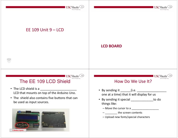
EE 109 Unit 9 LCD LCD BOARD 9.3 9.4 How Do We Use It? The EE - - PowerPoint PPT Presentation

ee 109 unit 9 lcd
SMART_READER_LITE
LIVE PREVIEW

EE 109 Unit 9 LCD LCD BOARD 9.3 9.4 How Do We Use It? The EE - - PowerPoint PPT Presentation

9.1 9.2 EE 109 Unit 9 LCD LCD BOARD 9.3 9.4 How Do We Use It? The EE 109 LCD Shield The LCD shield is a _____________________ By sending it ______(i.e. _________________ LCD that mounts on top of the Arduino Uno. one at a time)


slide-1
SLIDE 1

9.1

EE 109 Unit 9 – LCD

9.2

LCD BOARD

9.3

The EE 109 LCD Shield

  • The LCD shield is a _____________________

LCD that mounts on top of the Arduino Uno.

  • The shield also contains five buttons that can

be used as input sources.

5 Button Inputs

9.4

How Do We Use It?

  • By sending it ______(i.e. _________________
  • ne at a time) that it will display for us
  • By sending it special _____________to do

things like:

– Move the cursor to a __________________ – ________ the screen contents – Upload new fonts/special characters

slide-2
SLIDE 2

9.5

How Do We Communicate?

  • The LCD uses a "parallel" interface (4-bits sent per transfer) to

communicate with the µC (Note: µC => microcontroller)

  • Data is transferred 4 bits at a time and uses 2 other signals

(Register Select and Enable) to control _________ the 4-bits go and _________ the LCD should capture them Uno

Data lines

D7 D6 D5 D4 D8 D9

Register Select Enable

LCD

EE 109 is fun! Walk your bike!

9.6

Commands and Data

  • LCD contains ___________ registers which it

uses to control its actions: Command and Data

  • A Register Select (RS) signal determines which

register is the destination of the data we send it (RS acts like an address selector)

– RS = ____, info goes into the command register – RS = ____, info goes into the data register

  • To perform operations like clear display, move

cursor, turn display on or off, write the command code to the command register.

  • To display characters on the screen, write the

ASCII code for the character to the data register.

Command Code Clear LCD 0x01 Curser Home (Upper-Left) 0x02 Display On 0x0f Display Off 0x08 Move cursor to top row, column i 0x80+i Move cursor to bottom row, column i 0xc0+i

9.7

How Do We Communicate?

  • To transfer data we send it in two groups of 4

– First the ________ 4-bits followed by the _________ 4-bits

  • RS=0 sets the destination as the command reg.
  • RS=1 sets the destination as the data reg.

Uno

Data lines

D7 D6 D5 D4 D8 D9

Register Select Enable

LCD

0011 1001 Command Reg. Data Reg. 1 Address (Reg. Select) Display HW

7 6 5 4 3 2 1 0 1 1 1 1 1st Transfer 2nd Transfer

9.8

How Do We Communicate?

  • To transfer data we send it in two groups of 4
  • RS=0 sets the destination as the command reg.
  • RS=1 sets the destination as the data reg.

Uno

Data lines

D7 D6 D5 D4 D8 D9

Register Select Enable

LCD

0011 0110 1001 0001 Command Reg. Data Reg. 1 Address (Reg. Select) Display HW

7 6 5 4 3 2 1 0 1 1

1

1

1

1st Transfer 2nd Transfer

slide-3
SLIDE 3

9.9

Another View

  • Data from the Uno is transferred by placing four bits on the data

lines (PD[7:4]).

  • The Register Select (RS) line determines whether the data goes

to the LCD’s "Command Register" or "Data Register"

– RS=0 => Command Register RS=1 => Data Register

  • The Enable (E) line acts as a _________ signal telling the LCD to

capture the data and examine the RS bit on the _____ transition

– Pulse must be held at 1 for at least 230ns according to LCD datasheet

0000 0101 0110

(PB0) RS (PD[7:4]) Data (PB1) Enable "0000 0101" sent to the command register in the LCD The first 4-bits of a transfer to the data register in the LCD

230 ns 230 ns 230 ns 9.10

Another View

  • Data from the Uno is transferred by placing four bits on the data

lines (PD[7:4]).

  • Whether sending info to the "command" or "data" register, the

LCD still wants a full byte (8-bits) of data so we must do 2 transfers

– We always send the upper 4-bits of the desired data first – Then we transfer the lower 4-bits

0000 0101 0110

(PB0) RS (PD[7:4]) Data (PB1) Enable "0000 0101" sent to the command register in the LCD The first 4-bits of a transfer to the data register in the LCD

230 ns 230 ns 230 ns 9.11

Who's Job Is It?

  • So who is producing the

values on the RS and Data lines and the 0-1-0 transition on the E line?

  • _______!! With your

___________ (setting and clearing _______ bits)

(PD0) This code would produce some voltage pattern like this on PD0 Note: The LCD connection doesn't use PD0, you'll need to modify this appropriately to generate the E signal

// Turn on bit 0 of PORTD PORTD |= 0x01 // Delay 1 us > 230ns needed _delay_us(1); // Turn off bit 0 of PORTD PORTD &= ~(0x01) 9.12

Other LCD Interface

  • Other LCD devices may use

– Only one signal (a.k.a. serial link) to communicate between the µC and LCD

  • This makes wiring easier but requires more complex

software control to "serialize" the 8- or 16-bit numbers used inside the µC

– 8-data wires plus some other control signals so they can transfer an entire byte

  • This makes writing the software somewhat easier
slide-4
SLIDE 4

9.13

LCD LAB PREPARATION

9.14

Step 1

  • Mount the LCD shield on the

Uno without destroying the pins

  • Download the “test.hex” file

and Makefile from the web site, and modify the Makefile to suite your computer.

  • Run “make test” to download

test program to the Uno+LCD.

  • Should see a couple of lines of

text on the screen.

9.15

Step 2

  • Develop a set of functions that will

abstract the process of displaying text on the LCD

– A set of functions to perform specific tasks for a certain module is often known as an _______ (application programming interface) – Once the API is written it gives other application coders a nice simple interface to do high-level tasks

  • Download the skeleton file and

examine the functions outlines on the next slides

9.16

LCD API Development Overview

  • Write the routines to control the LCD in layers

– Top level routines that yours or others code can use: _____________________, __________________, etc. – Mid level routines: write a byte to the command register, write a byte to the data register – Low level routines: controls data lines and E to transfer a nibble to a register

  • Goal: Hide the ________________ about how the

interface actually works from the user who only wants to put a string on the display.

slide-5
SLIDE 5

9.17

High Level API Routines

  • init_lcd()

– Does all the steps to initialize the LCD – See the lab writeup and follow it exactly as written – Uses: writenibble(), writecommand(), delays

  • moveto(unsigned char row, unsigned char col)

– Moves the LCD cursor to “row” (1 or 2) and “col” (1-16) – Translates from row/column notation to the format the LCD uses for positioning the cursor (see lab writeup) – Uses: writecommand()

  • stringout(char *s)

– Writes a string of character starting at the current cursor position – Uses: writedata()

9.18

Mid-Level Functions

  • writecommand(unsigned char x)

– Send the 8-bit byte ‘x’ to the LCD as a command – Set RS to 0, send data in two nibbles, delay – Uses: writenibble()

  • writedata(unsigned char x)

– Send the 8-bit byte ‘x’ to the LCD as data – Set RS to 1, send data in two nibbles, delay – Uses: writenibble()

  • Could do as one function

– writebyte(unsigned char x, unsigned char rs)

9.19

Low Level Functions

  • writenibble(unsigned char x)

– Assumes RS is already set appropriately – Send four bits from ‘x’ to the LCD

  • Takes 4-bits of x and copies them to PD[7:4] (where we've

connected the data lines of the LCD)

  • Produces a 0-1-0 transition on the Enable signal

– Must be consistent with mid-level routines as to which 4 bits to send, MSB or LSB – Uses: logical operations (AND/OR) on the PORT bits

9.20

Step 3

  • Complete the LCD Lab after first

understanding how to use the buttons present

  • n the LCD shield

– Information about how to use the buttons is presented in the next slides

slide-6
SLIDE 6

9.21

LCD Shield Buttons

  • The LCD shield has 5 buttons
  • However, they do not produce 5

individual signals like you are used to from previous labs

  • They are configured in such a way

such that they sum together to produce a single ______________ which the shield connects to the A0 input of the Arduino

  • If the voltage is in _____________

we can infer that a particular button is being pressed

5 Button Inputs => 1 analog voltage

Uno

A0

9.22

LCD Shield Buttons

  • You can use the Arduino's _________

converter to sense when a button is pressed

  • Each button produces a certain

voltage when pressed and the default value of 5V when no button is pressed

  • The table to the right shows the

nominal voltages and 10-bit ADC result

– Note these are nominal and could be different so it would be best to just split the range evenly (e.g. to know the 'Up' button is pressed check if the 10-bit ADC results is between 104 and 308 )

Button Volts (V) Avg. 10-bit Value Right 0 V Up 1.0 V 208 Down 2.0 V 408 Left 3.1 V 624 Select 4.0 V 816 None 5V 1023

9.23

THE DEVIL IN THE DETAILS…

Ensuring the Enable pulse is long enough

9.24

Making Things Work Together

Does your code do the right thing?

  • Lab 6 required the program to generate an Enable (E) pulse.
  • Example: The writenibble() routine controls the PB1 bit that is

connected to the LCD Enable line.

PORTB |= (1 << PB1); // Set E to 1 PORTB &= ~(1 << PB1); // Clear E to 0

  • Creates a 0➞1➞0 pulse to clock data/commands into LCD.
  • But is it a pulse that will work with the LCD?
  • Rumors circulated that the E pulse had to be made longer by

putting a delay in the code that generated it.

  • Don’t Guess. Time to read the manual, at least a little bit.
slide-7
SLIDE 7

9.25

Making Things Work Together

Check the LCD controller datasheet

Timing Characteristics

  • RS
  • R/W

E DB0 to DB7

  • VIH1

VIL1

  • VIH1

VIL1 tAS tAH VIL1 VIL1 tAH PWEH tEf

  • VIH1

VIL1

  • VIH1

VIL1 tEr tDSW tH

  • VIH1

VIL1

  • VIH1

VIL1 tcycE VIL1 Valid data

Figure 27 Write Operation

9.26

Making Things Work Together

Check the generated code

  • Can check the code generated by the compiler to see what is

happening.

  • For the creation of the E pulse the compiler generated this

code:

SBI PORTB, 1 ; Set Bit Immediate, PORTB, bit 1 CBI PORTB, 1 ; Clear Bit Immediate, PORTB, bit 1

  • According to the manual, the SBI and CBI instructions each

take 2 clock cycles

  • 16MHz ⇒62.5nsec/cycle, so pulse will be high for 125nsec

9.27

Making Things Work Together

Check with the oscilloscope

9.28

Making Things Work Together

Extend the pulse

  • At 125nsec, the E pulse it not long enough although it might

work on some boards.

  • Can use _delay_us() or _delay_ms() functions but these are

longer than needed since the minimum delay is 1 us (=1000 ns) and we only need 230 ns

  • Trick for extending the pulse by a little bit:

PORTB |= (1 << PB1); // Set E to 1 PORTB |= (1 << PB1); // Add another 125nsec to the pulse PORTB &= ~(1 << PB1); // Clear E to 0

slide-8
SLIDE 8

9.29

Making Things Work Together

Better looking pulse

9.30

Making Things Work Together

Extend the pulse (geek way)

  • Use the “asm” compiler directive to embed low level

assembly code within the C code.

  • The AVR assembly instruction “NOP” does nothing, and takes

1 cycle to do it.

PORTB |= (1 << PB1); // Set E to 1 asm(“nop”::); // NOP delays another 62.5ns asm(“nop”::); PORTB &= ~(1 << PB1); // Clear E to 0

9.31

Making Things Work Together

Don’t guess that things will work

  • When working with a device, make sure you know what types
  • f signals it needs to see

– Voltage – Current – Polarity (does 1 mean enable/true or does 0) – Duration (how long the signal needs to be valid) – Sequence (which transitions comes first, etc.)

  • Have the manufacturer’s datasheet for the device available

– Most of it can be ignored, but some parts are critical – Learn how to read it

  • When in doubt ➔ follow the acronym used industry-wide:

RTFM (read the *!@^-ing manual)