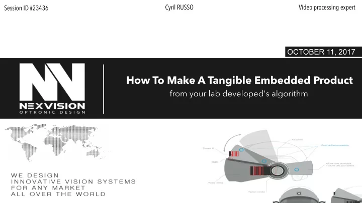
SLIDE 1 How To Make A Tangible Embedded Product
from your lab developed's algorithm
OCTOBER 11, 2017
Session ID #23436 Cyril RUSSO Video processing expert
SLIDE 2
INTRODUCTION
Nexvision is an European specialist in embedded electro-optics
system design
Our expertise includes optics, multispectral sensors, image processing and analysis, compression and streaming on FPGA, GPU and CPU, on several markets We design complete embedded system
SLIDE 3
SLIDE 4
CASE STUDY: VTOL GIMBAL [1/4]
One of the desired feature requirement:
1. Detect helideck from 2 nautical miles away 2. Track the detected helideck to help the autopilot plan the fight path 3. Detect obstacles on the computed route An advanced guimbal for situational awareness
SLIDE 5 CASE STUDY: VTOL GIMBAL [2/4]
Is it possible to achieve this requirement ? How to perform this task ?
Which algorithms ?
Typical process:
Which platform ? Environmental conditions ? How to test/assert the implementation ?
SLIDE 6 Resumes to... How to ft
SLIDE 8
PC GPU VS EMBEDDED GPU [obvious diff]
Processing power Power consumption Form factor Location of processing algorithms (CPU, GPU, ISP)
SLIDE 9
PC GPU VS EMBEDDED GPU [less obvious diff]
Managing the industrial image sensors (not MIPI) and their bandwidth Signal processing (pre/post processing and comp. offoading) Is an additional different sensor more effcient to simplify further processing?
SLIDE 10
PC GPU VS EMBEDDED GPU [less obvious diff]
FPGA based ISP for the other sensor types (linear, SWIR/Thermal/THz, beam forming radar, ...) High speed feedback loop and signal latency optimization Backing up processing results for subsequent error analysis and feedback reporting
SLIDE 11
INDUSTRIAL PRODUCT DESIGN PROCESS
Before starting the process
1. Profle the algorithm on a Jetson dev board 2. Does it run within the given latency budget ?
Yet it's a... Bad idea: To expect the input signal from the embedded system to match the lab's test sequences. Bad idea: Using “black boxes” Good idea: To specify type and format of the input signal (dynamic range, SNR, frame-rate)
SLIDE 12
STRATEGY FOR ALGORITHM FITTING
Is it possible to move part of it in the pre-processing part ? Rule of thumb: Ease of development: CPU > GPU > FPGA > ASIC Processing speed & dev cost: ASIC > FPGA > GPU > CPU Else => Required embedded power w/technical constraints (power consumption / weight / size / environment)
SLIDE 13 CASE STUDY: VTOL GIMBAL [3/4]
Tracking algorithm could not run in realtime with the selected 12MP image sensor Algorithm profling charged the feature point extraction code for half of the processing time Optimizing the algorithm more would have used too many time and gains were asymptotically decreasing. Instead, we moved the HOG computation code in the FPGA's ISP The GPU relaxed and we could focus on other algorithms
SLIDE 14 CASE STUDY: VTOL GIMBAL [4/4]
Which platform ? 3 IS + 2 FPGA + 3 Tegra K1 SOC
1. Tegra K1 because industrial temp condition 2. 2 GPU because aero safety requirement of independent algorithms 3. One FPGA to deal with 3 IS preprocessing and computing HOG
Which environmental conditions and how to test/assert the implementation ?
1. Build only one prototype that'll be used fight tests used to record test sequences and capture env conditions, vibration, exposure time, contrast, dynamic range in real conditions 2. Then build the product
SLIDE 15 INDUSTRIAL PRODUCT DESIGN PROCESS
Design of a frst electronic board (and mechanical structure) for a prototype Usually reuse IP as it saves dev. time and TTM Development of:
- 1. Hardware boards
- 2. Firmware for the ISP chip
- 3. Software stack for the CPU
- 4. Signal analysis stack for the GPU
- 5. Test/reporting stack for all components
SLIDE 16
TIME SAVING IN IND. PRODUCT DESIGN
Don't double spend your product development budget
1. Use the frst prototype to tests all the crazy ideas you have 2. Capture as much data as possible from all your sensors 3. Don't skip the input signal preprocessing step 4. But don't re-invent the wheel for the ISP code 5. No more 3+ steps development 6. Use your customers as beta testers, they love it "we'll see later" is a bad motto.
SLIDE 17 Usual process 2 steps process
SLIDE 18
CONCLUSION
No black box. Straight to the product. Real-world input signal. Early customer implication in project.
SLIDE 19
CONTACT
SLIDE 20