
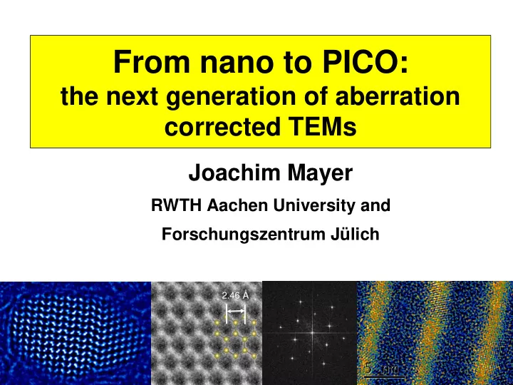
SLIDE 1
From nano to PICO:
the next generation of aberration corrected TEMs
Joachim Mayer
RWTH Aachen University and Forschungszentrum Jülich
2.46 Å
From nano to PICO: the next generation of aberration corrected TEMs - - PowerPoint PPT Presentation
From nano to PICO: the next generation of aberration corrected TEMs Joachim Mayer RWTH Aachen University and Forschungszentrum Jlich 2.46 Ernst Ruska-Centre for Microscopy and Spectroscopy with Electrons Cs-corrected protoype
RWTH Aachen University and Forschungszentrum Jülich
2.46 Å
Ernst Ruska-Centre for Microscopy and Spectroscopy with Electrons
FEI TITAN 80 – 300 (2006)
Cs-corrected protoype Cs-corrected Cs/Cc-corr.
Rose, Haider, Urban (1998)
m mm nm µm Å Hair Light Transistor Atom Comparison of Resolution Limits of Optical Instruments pm Electron wavelength x 100 x 100
Magnetic Lens Gaussian Image Plane Phase-Shift 500 correctors for spherical aberration installed worldwide
Chromatic Aberration two correctors for chromatic aberration (HRTEM) installed worldwide
2.46 Å
Lens
Image plane
Volkswagen Stiftung
Haider, Rose, Urban et al. Nature 392, 768 (1998)
P
Chromatic Aberration
Correction Principle: Wien Filter E B image plane
Harald Rose and Max Haider
Correction Principle: Crossed Electrostatic/Magnetic Quadrupoles
Harald Rose and Max Haider
828 mm, 470 kg, 160 channels
Chromatic Aberration
c c
PICO resolution
Fourier transform of CC and CS correct
Sub-Ångstrøm resolution at 80 kV Resolution improvement to 0.8 Å due to CC-correction
0.5 nm
Few- layer hexagon al boron nitride viewed along c- axis Haider et al, Ultramicroscopy 108 (2008) 167
PICO: atomic resolution at 50 kV
inverted positive phase contrast
2 nm
2.46 Å
Pd
9.37 nm-1
sample courtesy of U.Bangert, University of Manchester
9.8 nm-1 Au/C
1 Å
Catalytic Rh-Nanoparticles in Ionic Liquid on Graphene
Case study
PICO, U = 80 kV
Determination of the 3D shape of a nanoscale crystal with atomic resolution from a single image
Thust, NATURE MATERIALS | VOL 13 | NOVEMBER 2014
Experimental image Simulated image
Determined 3D atomic arrangement and displacements of atoms: atomically resolved view of the best-fitting 3D atomic arrangement for the sample region shown. Red spheres: fully
to highlight surface atoms. In the surface layers, brown spheres indicate formally half-occupied Mg sites, while cyan spheres indicate formally half-occupied O sites.
STEM
Electron energy loss spectrum
3
s s
c c
d
4 3
E del
2 del 2 d 2 s 2 c tot
Wide field of view: SrTiO3 <100>, hollow-cone EFTEM Ti L23
pre-edge 1 pre-edge 2 post-edge Ti-L23 map Sr-M map (pre-edge)
EFTEM Resolution & Cc-Correction
Delocalisation Cs Cc Diffraction
limit
limit Delocalisation Cs Cc Diffraction
Cc=1.4 mm Cc=10 μm W=50 eV W=10 eV
Cs corrected Cs and Cc corrected
As in Krivanek et al, J. Microsc. 180 (1995) 277
Pre edge 1 Pre edge 2 Si-L Map Post edge EFTEM, Si-L edge at 99 eV, energy window 40 eV 1.35 Å
Marc Heggen, ER-C
28
„Fuel-to-Power“
„Power-to-Fuel“
„Power-to-Storage“
PLB = post lithium batteries SOEC = solid oxide electrolyser cells SOFC = solid oxide fuel cells
Power to Fuel: Hydrogen Production
CdSe/CdS hybride particles: use as photo- catalysts for water separation CdSe: used for charge separation CdS: larger bandgap, charge transfer properties How do growth, surface and interface/defects depend on the choice of organic ligands?
Lothar Houben, Juri Barthel (ER-C) collaboration with M. Bar Sadan, S. Mangel, Ben Gurion University
H2 H2 O2
Stability of CdSe/CdS NP surfaces at 80 kV
PICO: Structural stability is given at 80 kV
focal series for residual aberration correction Focal series C1 = -15.6 nm ... 9.6 nm C5 = +3.5 mm, C3 = -10.6 μm
Surface coordination and termination
Cd S/Se Cd S/Se
1.4 Å
Focal series reconstruction
EFTEM of CdSe/CdS Nanoparticles (PICO)
HRTEM
a
zero loss filtered image
Se M45 jump ratio
Se M45
S L23, Se M23
b c
5 nm 5 nm
Se M edge jump ratio Se M45, Se M23 & S L23 EFTEM map
Lothar Houben in collaboration with M. Bar Sadan, S. Mangel, Ben Gurion University
E
I n t e n s i t y E
Characteristic edge EFTEM series
EFTEM ESI series of CdS/CdSe nanoparticles 80 kV, 35 eV - 235 eV, slit size 20 eV, step 10 eV
BMBF-project
Design Concept Vertical Transport
Si/SiO2-Superlattices: Fabrication by RPECVD at 250°C and Rapid Thermal Annealing at 900 to 1100°C
2.40 nm 2.64 nm 2.88 nm 2.74 nm
SiOx Si
4.95 nm 5.16 nm 4.90 nm
Sample: B. Spangenberg, H. Kurz, IHT, RWTH Aachen, TEM: A. Sologubenko, M. Beigmohamadi
Vertical Transport Lateral Transport
PICO Vertical Transport
Si/SiO2-Superlattices: Fabrication by RPECVD and Laser annealing
Sample: B. Spangenberg, H. Kurz, IHT, RWTH Aachen, TEM: M. Beigmohamadi
PICO: Energy Filtering TEM Si-L edge, 3 window meth.
Maryam Beigmohamadi, Jörg Jinschek